Device Testing
Required Pre Lab Reading: OP-Q, Tektronix Curve Tracer
OP-M, Capaciatnce-Voltage Measurements
Because of limited test equipment each group must schedule their testing
time independently. There are a large number of measurements to make, and
a great deal of data to analyze. You must work efficiently to get everything
done. In addition, make sure you read the post-lab questions now
and begin to think about them. You should answer these questions in
your final Lab Report (i.e. Lab Report 3); where you feel it is necessary
you may use any text books or reference works, but you MUST REFERENCE ALL
FORMULAS OR EXPLANATIONS YOU FIND IN THESE WORKS.
Note: Due to optical injection effects you must make all your measurements
in as nearly dark as possible. Make sure you turn the microscope illuminator
OFF before making any measurements.
CAUTION: THE MICROMANIPULATOR PROBE TIPS ARE VERY SHARP, AND VERY FRAGILE.
You MUST be extremely careful not to strike the needles against one another
or the substrate chuck. It is very easy to bend the tips, making them useless
for your measurements. The devices you are probing are fairly small, and
only sharp tips will be able to contact them. When you lower the tips to
contact your chips be very gentle; you should use the minimum amount of
tip pressure necessary to ensure contact.
Please use the sign-up sheets posted on the Lab doors to reserve the
curve-tracer and C-V system. Sign up in your own lab period slots if
possible; do not sign up for more than one period at a time on each system.
It will pay to get your data as soon as possible since there is a lot of
analysis to do.
Part I
Current-Voltage Measurements:
A) Diffused Resistors
On your n-type and p-type substrates measure:
1. For a good, long resistor measure the I-V curve of the resistor at low
voltages using PicoPete. Check at small voltages for linearity as V crosses
zero. Also check for linearity at large voltage using the curve tracer.
Make a qualitative sketch of your results. The substrate should be
floating for these measurements.
Repeat for a short resistor.
2. With the substrate and one resistor pad connected to ground, check I-V
curve at large voltages (with the curve tracer) for breakdown effects.
3. For the long resistors only measure the total resistance of:
i) Two resistors near the center of the chip.
ii) Two resistors near each edge of the chip. Make sure to note the location
on the chips of each resistor, along with its resistance.
* Use the probe station connected to the DMM for these measurements.*
B) Diffused Diode
On your n-type and p-type substrates measure:
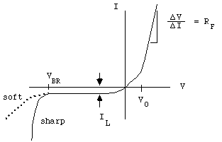
1. A complete I-V curve for one good diode. You should be able to extract
the following parameters: forward resistance, RF, breakdown voltage, VBR,
reverse leakage current, IL, and turn on voltage, VO. The breakdown voltage
is the voltage required for a leakage current of 10 uA. IL is measured at
VBR/2. See diagram on next page. Use PicoPete for these measuremnts.
I-V PARAMETERS FOR DIFFUSED DIODE
Note: You should remember which diode you probed, and use this same diode
for C-V measurements.
2. For two diodes near the center, and one near each edge, measure the breakdown
voltage VBR for each one. You will probably need to use the curve tracer
for this.
C) MOS Capacitors
On each of your samples check for leakage currents with a sweep of +
20V applied to the metal electrode. check three capacitors without guard
rings on each chip. Make sure you know which ones are either shorted or
leaky, if any. Use PicoPete for this.
D) MOSFET (Use PicoPete for this)
See OP-Q for measurement details. The MOSFET circuit and layout are illustrated
below:
see Lab Manual, p. Q-3 for connection diagram.
For each substrate:
1. Find the threshold voltage and transconductance of at least three MOSFET's
on each chip.
We use the following definitions:
Threshold voltage VT = VGS such that IDS = 100uA.
Transconductance gm:
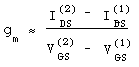
where
VGS(2) = gate voltage at IDS(2) = 200uA,
VGS(1) = gate voltage at IDS(1) = 100uA
Note: You can do all this very rapidly by measuring one device, then raising
all the probes using the z- axis adjustment ONLY, translating the substrate
to bring another device under the probes, and finally lowering the probes
into contact with the new device. Collect the raw data in a table.
2. For one good MOSFET on each chip obtain the family of curves describing
its operation. Use a gate voltage step of 0.1V, and a maximum saturation
current of about 0.5mA. Use the scope camera to record these.
Note: Your p-type substrates may yield MOSFET's that are conducting at Vgate
= 0, and may require the application of a negative gate bias to turn
them off. See the polarity guide table in the Lab Manual, p. Q-13.
Part II
Capacitance - Voltage Measurements:
A) Diffused Diode
On your n-type and p-type substrates:
1. Find a good diode by quickly measuring the capacitance- voltage curves
for several devices. A good diode should have its maximum capacitance at
V=0, and it should decrease with increasing REVERSE BIAS (see the introductory
section to OP-M). If you have already done your I- V measurements, use the
diode you used there.
Measure the C-V curve from OV to 10V (reverse bias - you may have to reverse
the LO and HI connections to the capacitance meter). Use a sweep rate no
faster than 0.1V/sec. Be careful about interpreting the meaning of HI and
LO on the C-V meter: The HI terminal is actually connected to the negative
side of the dc supply.
B. MOS Capacitors
On your n-type and p-type substrates:
1. C-V curve from -10V to +10V (where our convention is to measuring the
polarity of the Al electrode with respect to the substrate) for TWO different
capacitors (near the center of the chip) without guard rings. They should
agree to about 5%; if they do not, measure a third.
2. Repeat for capacitors with guard rings.
3. For the capacitors without guard rings, find the accumulation capacitance
for one capacitor near each edge of the chip. Make sure to note the location
on the chips of each capacitor, along with its capacitance. These results
will be used to check the oxide thickness uniformity of your chips.
C) MOSFET
1. C-V curve from -10V to 10V of the MOSFET gate on two different MOSFET's;
as above, if they differ by much more than 5%, do a third.
THIS CONCLUDES THE DEVICE MEASUREMENT SECTION
Questions to be answered in the third Lab Report:
A) Diffused Resistor
1. Using the geometry correction factors given in Ghandhi, p. 628, find
the sheet resistance RS of your resistors. Compare to the Rs from your MPT
chip measurements. Comment on the differences.
2. Compare the n-type resistor in a p-type substrate to a p-type resistor
in a n-type substrate. Why is there such a large difference in Rs between
the two?
3. Is the doping uniform across the face of the chip? Comment.
4. If one end of the resistor is connected to ground, and the substrate
is also connected to ground, what happens as you sweep the applied voltage
at the other end across zero? If this is a p-type resistor, can you apply
an arbitrarily large negative voltage to the resistor?
B) Diffused Diodes
1. C-V data analysis:
Recall
C = A[[epsilon]]ox/xd
where A = area of diode (get this from the Herman Masks) and xd = depletion
layer width.
Now using your C-V data, calculate xd vs. V, and plot on log-log paper.
Assuming
xd = BVn
find B and n from your plot. Does the plot deviate from
a straight line near V=0? Comment. From this, plot 1/C1/n vs
V on linear paper. Extrapolate this line to 1/C1/n = 0 to find
Vo, the built-in potential across the junction. Compare this to your measured
value from the turn-on voltage for the diodes. These calculations will
be done automatically by the computer when you use PicoPete and PCASP.
2. For the abrupt, one-sided junction we expect the value of n above
to be 1/2. Under these conditions the doping at xd is given by
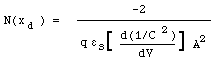
From your plot of 1/C2 vs V, the slope and this formula should
allow you to calculate the substrate doping, NB. If your value of n differs
significantly from 1/2, explain. How does this value of NB compare to the
substrate doping measured from your MPT chips? Why can't we obtain (much)
information about the diffusion doping profile with these measurements?
C) MOS Capacitors
1. From your "best" C-V curve:
i) find tox, the oxide thickness.
ii) find xdmax, the maximum depletion layer width.
2. From all your C-V measurements, find tox, and determine how uniform the
oxide thickness is across your chips. Compare the calculated oxide thickness
here to your MPT oxide measurements.
3. What affect does the guard ring have on your capacitors? Why is the maximum
capacitance for the capacitor with guard ring less than that for the non-guard
ring capacitor (look at the Herman masks)?
4. What would you expect the VT for a MOSFET to be based on your C-V curves?
Substitute this VT into the equations given in OP-M to find the excess surface
states charge Qss (give Qss in units of number density, i.e. #/cm2,
NOT IN COULOMBS/cm2). Note for a p-type substrate the basic equation
becomes:
VT = Qms + 2|[[phi]]F| + (Qb - QSS)/Co
Also be careful to remember the capacitances in these equations have been
normalized to capacitance per unit area. Comment on possible sources of
this excess charge.
D) MOSFET
1. What (and why) are the major differences between your p-channel and n-channel
devices?
2. Compare your measured VT's to what you would expect based on the C-V
curves for your gates.
3. The excess surface states charge is the cause of our relatively large
VT's; how might we identify the source of this charge?
4. Use the Herman mask diagrams to determine the MOSFET gate width, and
from that the transconductance per millimeter for your devices.