Return to the IC Fab Lab Manual Table of Contents
Trouble Shooting During Device Testing
The device testing done in our lab is one of the most difficult
parts of the class. This is because many of you are not accustomed to making
measurements of truly unknown quantities. As discussed in the lab report
section, we never really know what to expect from our fabrication process.
Because the range of electrical characteristics that can result from nonideal
fabrication is bewildering, you may feel overwhelmed by the data you collect
during the test phase.
STEP ONE: DON'T PANIC!!!!
STEP TWO: NEVER TAKE DATA BEFORE YOU UNDERSTAND EXACTLY WHAT YOU ARE
MEASURING!!
There are a number of very simple things you need to verify before making
a measurement:
Do you have the wires connected correctly between probes and test instrument?
to the substrate chuck? to the device itself?
These questions are not as simple as they may seem, and require that you
really understand how to hook up a device. For an I-V measurement, one way
to test the connections between probers and the test instrument is to try
to form a "short circuit" at the probe tips (touch them together!).
Since you know what the I-V curve of a short looks like (I hope), you can
check your connections. Now try an open circuit. These are simple tests,
but very important.
Once you have verified that you really have the right connections, what
do you do if the device doesn't work? Obviously, I would ask: "How
doesn't it work?" Is it a short? An open? A resistor when you expected
a diode? A diode when you expected a resistor? This could go on forever,
but you should be asking yourself these kind of questions. You really have
to think about how devices work, but don't get too lost in elaborate semiconductor
physics.
Another important thing to realize is the order of your testing is important!
For instance, C-V measurements rarely make sense for devices that pass a
large amount of dc current.
* For MOS capacitors this means an I-V measurement should be done to insure
the caps are not leaky before any C-V measurements are attempted.
* For diodes, this means an I-V measurement must be performed to insure
C-V is done only over a voltage range where the reverse bias leakage current
is small.
Note you cannot even make I-V measurements unless you know you have good
ohmic contacts to the silicon. A good way to check this would be an I-V
measurement between the backside and front-side "substrate" contacts
to the chip. What does it mean if this gives a diode-like curve? A resistor-like
curve? What should it be?
If a device doesn't work the way you "expected," you need a strategy
to determine why it didn't work. For a MOSFET, the most useful approach
is to look at the various components that make up a MOSFET. For instance,
the source-substrate and drain-substrate form p-n junction diodes. A good
check would be to measure the I-V curve of these diode "sub-components."
What would happen to the MOSFET I-V curves if these junctions are leaky?
What would happen to the curves if your source/drain contacts to the silicon
exhibit very high resistance? Even if everything is fine with the device,
you may still have hooked it up wrong; for instance, what would the I-V
curve look like if you select the "wrong" polarity (with respect
to the substrate) for the drain bias?
I recommend the following procedures:
* Before doing any C-V measurements, do I-V testing on the devices to
ensure that leakage currents are small.
* Don't collect large amounts of "strange" looking data, expecting
you will be able to figure it out later. Think about it while you are
measuring, and try different tests to check for obvious errors (mis-connections,
leaky diodes, bad contacts, etc.).
* Do C-V on MOS capacitors before doing I-V on your MOSFETs. This
will allow you to determine what gate biases are needed to operate the MOSFETs.
* Think about the relationships between data seen in one type of device
to other devices. How does diode I-V data help you understand MOSFETs? How
does MOS cap C-V data help you understand the MOSFETs? What does resistor
behavior tell you about diodes, and vice versa?
* THINK!!!
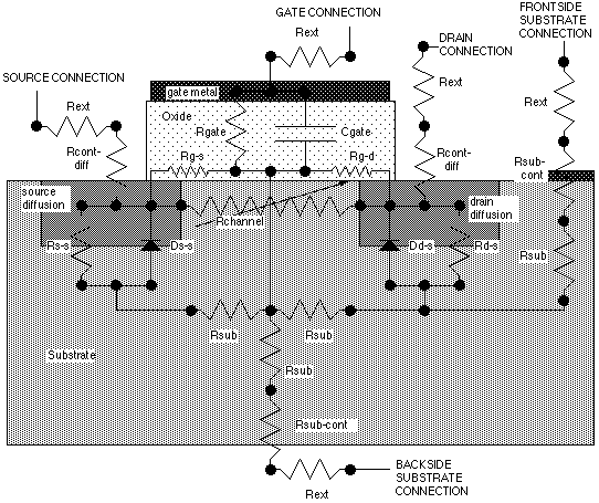
How to find a "GOOD" MOSFET:
The following procedure could be used to ensure that you find a "good"
MOSFET (or alternatively, find out what part of your MOSFET does not
work). This sequence is designed to identify the sub-components of a MOSFET,
as shown below. To measure a working MOSFET all the sub-components
must work properly.
The sub-components are defined as follows:
Rext: external parasitic resistances due to probe cables and connectors
Rsub-cont (frontside and backside): contact resistance between Al metallization
and the undiffused (substrate) areas of chip
Rgate: resistance of gate oxide "insulator" to substrate under
gate
Cgate: capacitance of gate oxide
Rg-s and Rg-d: resistance of gate oxide "insulator" to source
and drain diffused regions (respectively) under gate
Rchannel: gate voltage-controlled effective resistance of the channel region
Rcont-diff: contact resistance between Al metallization and the diffused
areas of chip
Ds-s and Dd-s: diodes formed by source-substrate and drain-substrate p-n
junctions
Rs-s and Rd-s: reverse-bias leakage "resistance" of source-substrate
and drain-substrate p-n junctions
Rsub: substrate resistance
Most of us would recognize the essential feature of a MOSFET as the channel,
whose equivalent resistance Rchannel (i.e., the relation between the source-drain
current and the source-drain voltage) is controlled by the voltage applied
between the gate and the substrate. These characteristics are represented
by the conventional family of Ids-Vds vs Vg curves for the device. However,
for our "home-made" MOSFETs, the characteristics of all the other
sub-components must also be verified. The various structures fabricated
with the Holberg mask set should allow you to check each part of the device
in turn.
If you understand how a MOSFET works, then you should know what an approximately
"proper" value is for each. Here is a check list; indicate with
a check mark what value you should get for each sub-component:
| Sub Components | Resistance | |||
open | high | low |
short | |
| Rext | ||||
| Rsub-cont | ||||
| Rgate | ||||
| Rg-s | ||||
| Rg-d | ||||
| Rcont-diff | ||||
| Rs-s | ||||
| Rd-s | ||||
| Rsub | ||||
For the diode sub-components (assuming the substrate is the grounded reference), we should also determine which polarity is forward bias, and which is reverse. In the following table, indicate whether a positive (+) or negative (-) voltage should be applied to the diffusion contact to achieve the indicated bias condition. Also indicate whether the junction should exhibit a high or low resistance under the given bias condition.
| sample | forward bias |
reverse bias | ||
polarity |
resistance |
polarity |
resistance | |
| p-type substrate, n-type diffusion | ||||
| n-type substrate, p-type diffusion | ||||
Now that you have filled in the tables, you know what to look for
as you take data. As I said earlier, it is extremely important to
examine your data as you take it to see if it is reasonable. The
rest of our procedure will be designed to measure each sub-component, ideally
one at a time. Some components are almost always connected together, so
we may need to be creative in trying to isolate their individual contributions
to the measurements.
It is also critical to determine whether a measurement made on one device
can be assumed to hold for another, i.e. we need to check for uniformity.
For instance, if you find that one p-n diffused diode is "OK,"
can you assume all the MOSFET source-substrate and drain-substrate
p-n junctions are also OK? You need a quick strategy to check for "qualitative
uniformity." For this example, one way is to check several p-n diodes;
they must ALL have I-V curves which are qualitatively similar. If
even one is "bad," since your sample was probably small,
the chance of another p-n junction being bad is HIGH! In such a case you
will have to individually qualify a single MOSFET, and make all your
measurements on that SAME device.
MOSFET QUALIFICATION PROCEDURE:
STEP 1: Check Rext: Obviously, you have to make sure the hook-up between
measurement instrument and device. You should do this both visually and
electrically (for instance, by either shorting or opening appropriate connections).
STEP 2: Check Rsub-cont: We must have an ohmic contact to the substrate
to make any further measurements. One way is to try to measure an I-V curve
between the frontside and backside substrate contacts. It should be linear
through the origin, NOT a Schottky-like curve.
STEP 3: Check Rcont-diff: This is actually very hard to do quantitatively.
We have one device on the chip (in the lower center area of the die shown
on p. 38) called a Kelvin structure which is specifically designed for contact
resistance measurement. At present we are not using this device, but instead
use the diffused resistors to estimate Rcont-diff. The I-V measurements
discussed on p. 26, along with the analysis on pp. 31-32 should be used
estimate Rcont-diff. You should also do a quick check now to see
if the diffusion sheet resistance extracted from the resistors compares
well with your four-point probe measurements made on the MPTs.
STEP 4: Evaluate p-n junctions: This should help establish the characteristics
of Ds-s and Dd-s (and thereby Rs-s and Rd-s). Start with I-V measurements
on the diffused diodes, pp. 26-27. In addition, set up to measure I-V between
the source of your target MOSFET and the substrate; it should look similar
to your diode curves. Same thing for the drain-to-substrate I-V. These
measurements can be made with the curve tracer.
STEP 5: Check Rgate, Rg-s, and Rg-d: Here we want to determine if gate
oxide leakage is a problem. Start with I-V measurements of your MOS Caps,
p. 27, done using PicoPete. Also check your target MOSFET, measuring I-V
between the gate and substrate, gate and source, and gate and drain.
Assuming all the measurements made above are sensible, we are now ready
to progress to C-V measurements
STEP 6: Check Cgate: Start by measuring the C-V characteristics of a MOS
Cap which I-V has shown to have low leakage. See section B, pp. 29-30. Make
sure you look at more than one, and determine the gate voltage range over
which the MOS Cap goes from accumulation to depletion. This should establish
the polarity of the threshold voltage Vt, and the range over which Vg should
be swept when you go back to I-V measurements of the MOSFET.
STEP 7: You are now ready (finally) to measure the family of Ids-Vds versus
Vg curves which characterizes your MOSFET. See pp. 27-29. Please make sure
to save at least one set of curves for your lab reports. Also make sure
to make the transconductance measurement.