Microelectronics Fabrication
Teaching Laboratory
Laboratory Manual
Spring, 1985
Rev 1: Fall, 1985; Rev 2: Spring, 1986; Rev 3: Fall, 1986
Rev. 4: Spring, 1987; Rev 5 Fall, 1987; Rev 6 Fall, 1988; Rev. 7 Fall 1989;
Rev. 8 Spring 1990; Rev. 10 Fall 1990; Rev. 11 Fall 1991; Rev. 12 Fall 1993
by
Dean P. Neikirk
Department of Electrical and Computer Engineering
University of Texas at Austin
Austin, TX 78712-1084 USA
tel (512)471-4669 or 471-8549
Preface
The Microelectronics Fabrication Laboratory has now been in
operation here at UT for eight years,; even so, it is still a lab course
which requires constant updating. This course has a number of objectives,
chief among them your exposure to basic silicon device processing. You will
be required to make use of information from many areas: solid state physics,
chemistry, electrical engineering, and computer science. Regardless of your
future intentions, we feel the material covered in lecture, and your experiences
in the lab, will be very valuable. The use of integrated circuits is pervasive,
and knowledge of how they are made is an important compliment to your knowledge
of how they can be used.
This laboratory is a synthesis of the work of a number of people. Similar
laboratories at Caltech (under the supervision of Prof. Jim McCaldin and
Prof. David Rutledge) and at the University of Illinois (originally developed
by Prof. Ben Streetman) have provided both inspiration and guidance. Industrial
support has been provided by Bell Laboratories, Advanced Micro Devices,
Motorola, and Texas Instruments. Both TI and Monsanto have provided silicon
wafers for our use. The Semiconductor Research Corporation has also provided
generous support for the development of our new mask set. The technical
staff (under the supervision of Mr. Harold Traxler and Marty Ringuette)
has provided invaluable assistance in setting up and maintaining the lab
equipment. The help of Philip Cheung, Doug Miller, Jeff Meitz, Stu Wentworth,
Carl Kyono, Doug Holberg, and Garrett Neaves in designing the experiments
is also gratefully acknowledged.
This lab is quite different from any other of the labs in your ECE curriculum.
The processing we do is very complicated, and there will be frequent, and
often very subtle, problems associated with it. You must be very patient
and methodical at all times. Since we have essentially only one set
of equipment, you must also be very careful. The lab is constantly evolving,
and there will be changes throughout the term as we get more equipment,
develop new experiments, and think of better procedures. Please feel free
to make suggestions that you think will help improve the lab.
Dean Neikirk
Last update to this html file: April 24, 1997.
Table of Contents and link to full lab manual
Filename page
I.    Introduction                              INTRO
      A. Lab Notebooks and Reports                                          0-6
      B. Grading                                                            0-7
      C. Safety                                                             0-8
			University of Texas Lab Safety Manual
II.   Experiments
      Introduction                              FABINT                      1
      Lab Schedule                                                          5
      Process Flow Summary                                                  6
      Processing Description                    PROCESS                     8
      Laboratory Report Guidelines              REPORTS update              19
      Result Summary Tables                                                 22-24
      Device Testing                            TEST89                      25
      Holberg Mask Set                          MASKS                       35
      Device Tests Trouble Shooting             TROUBLE                     48


II.   Operating Procedures
      A. High Temperature Furnaces              FURNAC                      A-1
      B. Wet Oxidation                          WETOX                       B-1
      C. Dry Oxidation                          DRYOX                       C-1
      D. Boron Pre-Deposition                   BPREDP                      D-1
      E. Phosphorus Pre-Deposition              PPREDP                      E-1
      F. Drive In Furnace                       DRIVE                       F-1
      G. Vacuum Evaporation                     VACEVP                      G-1
      H. Four Point Probe                       4PTPR                       H-1
      I. Hot Point Probe                        HOTPR                       I-1
      J. Wafer Cleaning                         CLEAN                       J-1
      K. Plasma Ashing                          PLASMD                      K-1
      L. Photolithography                       LITHO                       L-1
      M. Capacitance-Voltage Measurements       CVMAN                       M-1
                                                PCASP CV                    M-7
      N. Junction Depth Measurements            JUNCTD                      N-1
      O. Mask Aligners                          MCROTCH                     O-1
      P. Hydrofluoric Acid Etching              HFETCH                      P-1
      Q. Tektronix, Digital Curve Tracers       TEKCT                       Q-1
                                                PCASP IV                    Q-14
      R. Ellipsometer                           ELLIP                       R-1
      S. Microscopes, Line Measurements         MCSCRP                      S-1


IV.     Data Sheets                                                      page
        Aluminum etch                                                    IV-1
        Buffer - HF                                                      IV-2
        Photoresist                                                      IV-3
        PR Stripper                                                      IV-9
        BN Wafer data sheet                                              IV-13
        P Wafer data sheet                                               IV-15


V.   Physical Constants                                                  page
     Resistivity vs. Doping                                              V-1
     Kennedy & O'Brien Curves                                            V-2
     Nomograph for Abrupt p-n Junctions                                  V-3
     Physical Constants and Energy Conversions                           V-4


VI.Material Safety Data Sheets                                          page

Introduction                                                            VI-1
Acetone                                                                 VI-6
TCA                                                                     VI-8
Photoresist                                                             VI-10
HMDS (used in PR adhesion promoter)                                     VI-12
Hydrogen Peroxide                                                       VI-14
Hydrochloric Acid                                                       VI-16
Sulfuric Acid                                                           VI-18
Concentrated Hydrofluoric Acid                                          VI-20
Buffered Hydrofluoric Acid                                              VI-22
Aluminum Etch, Transene type A                                          VI-25
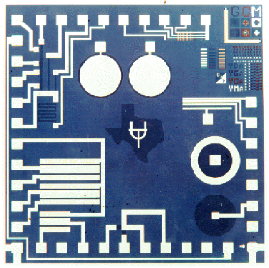
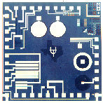
Holberg Mask Set
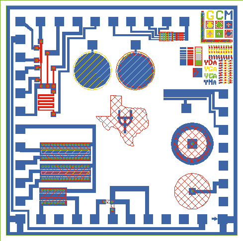
This section describes in detail the functions of the Holberg Mask Set,
shown with all four layers overlaid in Fig. 1, p. 38, and level-by-level
in Fig 2a-2d, pp. 39-42. Each functional block on the chip is discussed
separately. These blocks are:
i) Alignment, resolution, and registration patterns
ii) Metal step coverage and leakage patterns
iii) Diffused resistor and contact resistance test structures
iv) Diffused diodes
v) MOS capacitors
vi) Thick and thin oxide MOSFETs
Alignment, resolution, and registration patterns
The purpose of this part of the chip is to allow accurate alignment
of each mask level to preceding levels already patterned, as well as to
evaluate the accuracy of the alignment and the resolution of both lithographic
and etching processes. The area in the upper right corner of the chip (Fig.
1) is used for these purposes, and is shown level by level in Fig. 2a-2d.
Figure 3 (p. 43) shows a 200x, four level composite view of this region
of the chip.
Figure 4 (pp. 44-45) shows a diagram to illustrate how the registration
verniers are used to determine mis-alignment. In Mask Level 1 (Diffusion,
Fig. 2a) windows are opened to provide the center part of the verniers;
each subsequent level patterns bars on either side of the Level 1 pattern.
Misalignment is determined by finding the outer and inner boxes which line
up, and counting how many boxes from the end this occurs at. Each box from
the end corresponds to 1 um misregistration.
Diffused resistor and contact resistance test structures
The purpose of this part of the chip is to allow us to measure the sheet
resistance due to our diffusions, as well as to find contact and bend resistance
corrections. The area in the upper left corner of the chip (Fig. 1) is used
for these purposes, and is shown level by level in Fig. 2a-2d. Figure 5
(p. 46) shows a 100x, three level composite (diffusion: Level 1; contact:
Level 3; and metal: Level 4) view of this region of the chip.
There are four basic structures in this region. Two straight resistors,
one short (R1) and one long (R2), are used to find sheet and contact resistances.
Another serpentine resistor (R3) is used to find the equivalent size and
resistance of bends. The last structure allows four point measurement of
sheet resistance, to help remove contact resistance problems from the measurements.
See the TEST section, p. 31 for more details.
Diffused diodes
The purpose of this part of the chip is to allow us to evaluate a diffused
p-n junction diode. The region in the lower right corner of the chip (Fig.
1) is used for this purpose, and is shown level by level in Fig. 2a-2d.
There are two diodes of identical size, the top device also having a field
relief plate over the oxide covering the surface p-n junction.
MOS capacitors
The purpose of this part of the chip is to allow us to evaluate the
quality of our gate oxides. The region in the upper center of the chip (Fig.
1) is used to make two MOS capacitors at the same time we grow the gate
oxide for our MOSFETs. This area is also shown level by level in Fig. 2a-2d.
There are two capacitors of equal metal plate and thin oxide areas. The
right device, however, also has a diffused guard ring around the perimeter
of the capacitor.
Thick and thin oxide MOSFETs
The purpose of this part of the chip is fabricate two MOSFETs with different
gate lengths, as well as a thick oxide MOSFET to help evaluate the quality
of our field oxide. The area in the bottom left corner of the chip (Fig.
1) is used for these purposes, and is shown level by level in Fig. 2a-2d.
Figure 6 (p. 47) shows a 100x, four level composite view of this region
of the chip. The upper MOSFET (Device 1) has a longer channel than the device
below it (Device 2). All three MOSFETs share a common source connection
through the upper-most pad shown in Fig. 6.
Critical Mask Dimensions:
MOSFET channels:
Device 1 800um x 30um
Device 2 800um x 20um
MOS cap w guard ring: 600um diam.
MOS cap w/o guard ring: 550um diam.
Diode diffusion diam.: 550um
Diffused resistors (straight):
Device 1 250um (l) x 25um (w)
Device 2 500um (l) x 25um (w)
Registration verniers: 1um increments
Resolution bars:
   line     line         following           line     line        following
  number                   space            number                space
    1          2 um     2 um
    2          2 um     3 um                  8       10 um       10 um
    3          3 um     3 um                  9       15 um       15 um
    4          3 um     5 um                  10      15 um       15 um
    5          5 um     5 um                  11      20 um       20 um
    6          5 um     5 um                  12      20 um       20 um
    7         10 um     10 um                 13      25 um       25 um
                                              14      25 um
Contact Windows:
Diffusion area: 50um x 50um
Oxide window size (metal/semiconductor contact area):
25um x 25um
(click
the image for an enlarged view (about 134K))

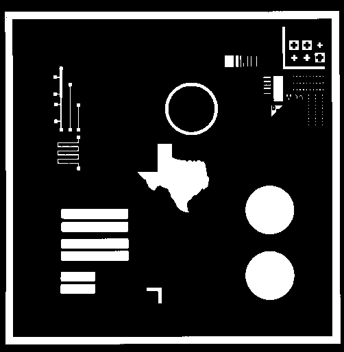
Figure 1: Composite drawing of the Holberg Mask set.
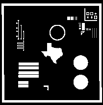
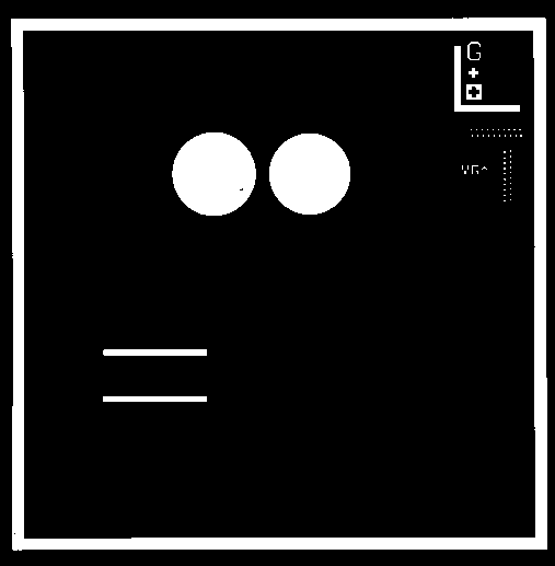
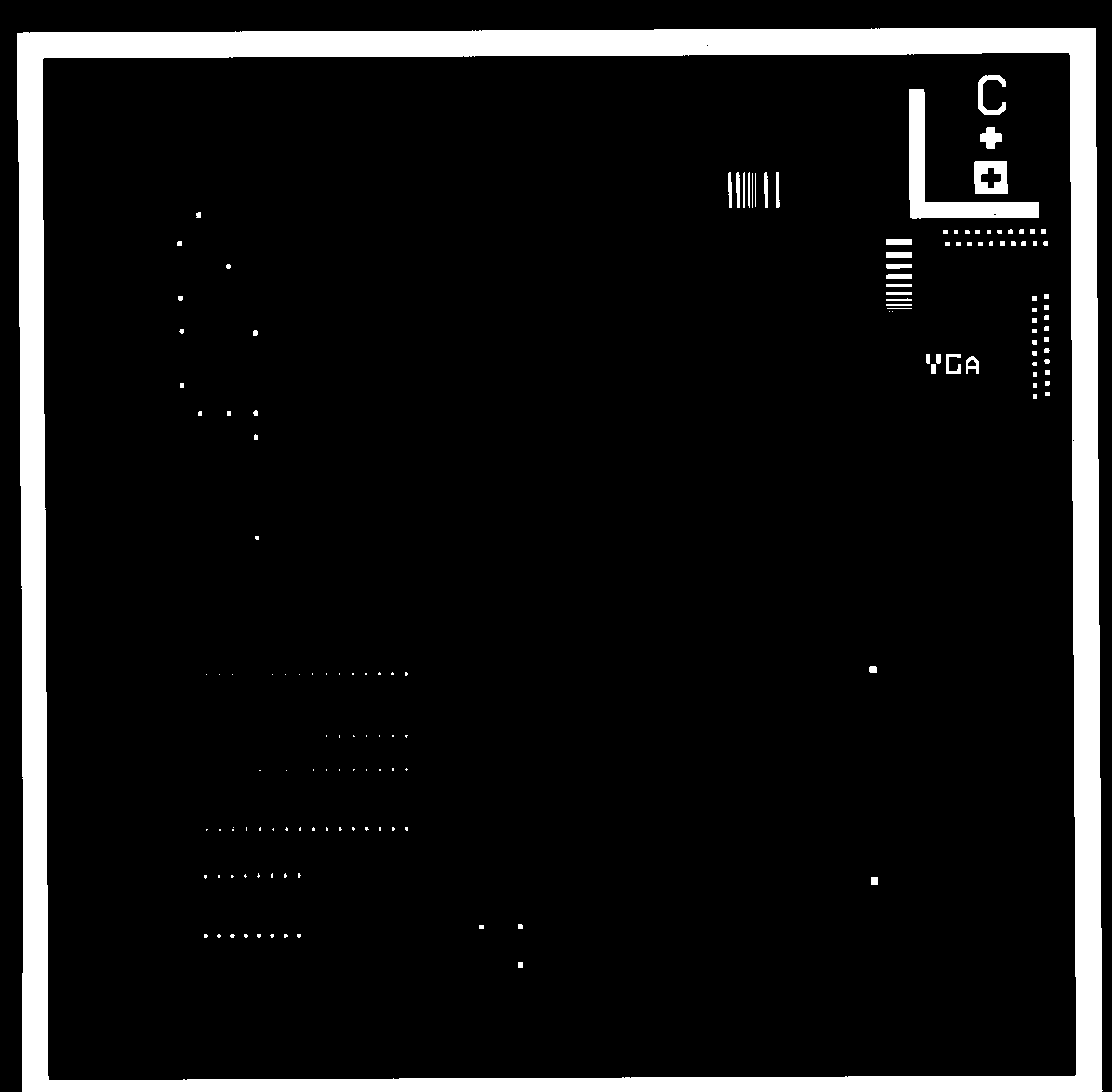
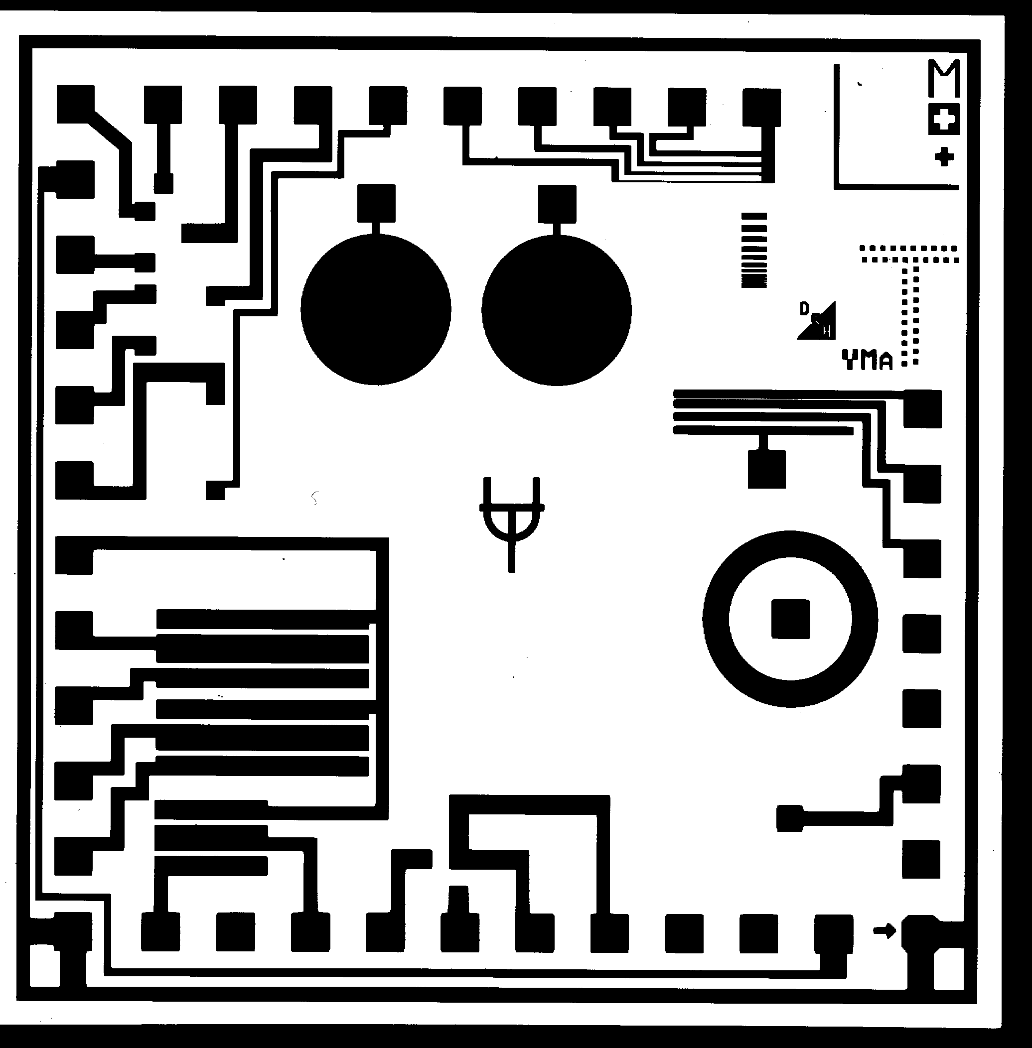
Figure 2a: Holberg Mask Level 1, Diffusion
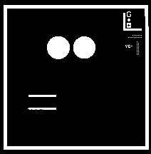
Figure 2b: Holberg Mask Level 2, Gate

Figure 2c: Holberg Mask Level 3, Contacts
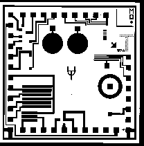
Figure 2d: Holberg Mask Level 4, Metal