A new quasi-static model for Schottky-contacted coplanar waveguide (CPW) on a semiconductor substrate is shown. Comparison between experimental measurements for a CPW on a GaAs epilayer and calculations show excellent agreement. The new model includes the effect of the finite resistance of the undepleted epilayers under the CPW electrodes [1,2].
Introduction: Coplanar waveguide (CPW) on semiconducting substrates has been extensively studied for possible use in phase shifting applications. The most common structure consists of CPW electrodes Schottky-contacted to a doped semiconducting layer on a semi-insulating substrate [3]. Two main techniques for the control of the propagation constant in such CPWs have been used: optical control [4] and voltage control [5-8]. For both cases, models of the behavior of the CPW are usually based on slow-wave effects. Here we report a quasi-static model for Schottky-contacted CPWs that is in excellent agreement with experimentally measured data over a wide range of frequency and bias conditions. While past models have emphasized the impact of depletion layer capacitance on the slow wave effect, we show that significant sensitivity to bias voltage is induced by resistance in the epi layer.
Model: A cross-sectional drawing of a Schottky-contacted CPW is shown in Fig. 1. The CPW center conductor is 2a wide, the gap between center conductor and ground plane is
where the superscript n is either gp, gap, or cntr, for the region under the ground plane, in the gap between electrodes, or under the center conductor, respectively. The epi layer is tepi thick, with conductivity [[sigma]]epi, and the bias-dependent depletion layer is hn thick. For simplicity, we have assumed a single, uniformly doped epitaxial layer, on a high resistivity substrate with residual sheet resistance
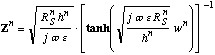 (2)
(2)where [[omega]] is the angular frequency, [[epsilon]] is the dielectric constant of the epi layer, n is either gp or cntr, and wn is the width of the region (
where Rgap is the total gap region resistance,
The propagation constant can be very sensitive to bias voltage when either hgp or hcntr are close to the total epi layer thickness tepi (i.e., the bias voltage has nearly depleted the epi layer) since small changes in bias induce very large changes in RS (even though h, and therefore the depletion layer capacitance, changes very little), inducing large changes in Ytot. This also explains the extreme sensitivity to optical illumination when biased near full depletion [12], since very low levels of illumination can induce large changes in RS.
Results and Conclusions: To verify the accuracy of this model, measurements have been made on coplanar waveguide fabricated on doped GaAs layers grown by molecular beam epitaxy on semi-insulating (SI) GaAs wafers. The epi layer consisted of a 1.5 um thick n-type (4 x 1015 cm-3) GaAs layer, a 0.1 um thick AlAs layer, and finally a 0.2 um thick GaAs undoped buffer layer. Accounting for Fermi level pinning at the SI substrate interface, the effective epi layer thickness used in eq. 1 is tepi = 1 um. In the gap region, Fermi level pinning also depletes 0.5 um from the front surface, so hgap = 0.5 um. The center conductor half-width a is 5 um, the gap
Acknowledgments: This work was sponsored in part by the Joint Services Electronics Program under grant number AFOSR 49620-92-C-0027 and the Advanced Research Projects Agency ASEM program.
References
1. M. S. Islam, E. Tuncer, and D. P. Neikirk, "Accurate Model for Schottky-Contacted Coplanar Waveguide Including Finite Epilayer Resistance Effects," Electron. Lett., vol. 30, pp. 712-713, 1994.
2. S. Islam, "Modeling and Experimental Studies of Schottky-Contacted Coplanar Waveguide Transmission Lines on Semiconductor Substrates," 1994, PhD, The University of Texas at Austin.
3. H. Hasegawa and H. Okizaki, "M.I.S. and Schottky slow-wave coplanar striplines on GaAs substrate," Electron. Lett., vol. 13, pp. 663-664, 1977.
4. P. Cheung, D. P. Neikirk, and T. Itoh, "Optically Controlled Coplanar Waveguide Phase Shifters," IEEE Trans. Microwave Theory Tech., vol. 38, pp. 586-595, 1990.
5. R. E. Niedert and C. M. Krowne, "Voltage Variable Microwave Phase Shifter," Electron. Lett., vol. 21, pp. 636-638, 1985.
6. C. M. Krowne and R. E. Niedert, "Slow wave monolithic variable phase shifter with operation into the millimeter wave wavelength regime," Int. J. Infrared Millimeter Waves, vol. 7, pp. 715-728, 1986.
7. C. M. Krowne and E. J. Cukauskas, "GaAs Slow Wave Phase Shifter Characteristics at Cryogenic Temperatures," IEEE Trans. Electron Devices, vol. ED-34, pp. 124-128, 1987.
8. V. M. Hietala, Y. R. Kwon, and K. S. Champlin, "Broadband Continuously-Variable Phase-Shifter Employing a Distributed Schottky Contact on Silicon," Electron. Lett., vol. 23, pp. 675-677, 1987.
9. J. H. Wiley and G. L. Miller, "Series Resistance Effects in Semiconductor CV Profiling," IEEE Trans. Electron Devices, vol. ED-22, pp. 265-272, 1975.
10. J. D. Wiley, "C-V profiling of GaAs FET films," IEEE Trans. Electron Devices, vol. ED-25, pp. 1317-1324, 1978.
11. M. S. Islam, E. Tuncer, and D. P. Neikirk, "Calculation of Conductor Loss in Coplanar Waveguide using Conformal Mapping," Electron. Lett., vol. 29, pp. 1189-1191, 1993.
12. M. S. Islam, A. J. Tsao, and D. P. Neikirk, "GaAs on Quartz Coplanar Waveguide Phase Shifter," IEEE Microwave and Guided Wave Lett., vol. 1, pp. 328-330, 1991.
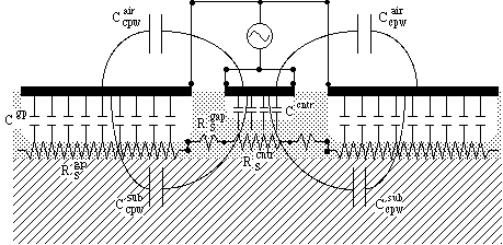 Figure 1: Schottky-contacted
coplanar waveguide on an epitaxial layer. Depletion regions under the electrodes
produce distributed capacitance, while the undepleted epi layer produces
a distributed resistance.
Figure 1: Schottky-contacted
coplanar waveguide on an epitaxial layer. Depletion regions under the electrodes
produce distributed capacitance, while the undepleted epi layer produces
a distributed resistance.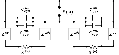 Figure 2: Equivalent
circuit for the shunt admittance per unit length of the coplanar waveguide.
Figure 2: Equivalent
circuit for the shunt admittance per unit length of the coplanar waveguide.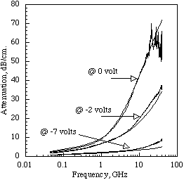 Figure 3: Measured
(solid lines) and modeled results (dashed lines) for attenuation constant
at 0 V, 2 V reverse bias on center conductor, and 7 V reverse bias on center
conductor; at 7 V the epilayer is fully depleted, so hcntr is
taken to be the full SI substrate thickness.
Figure 3: Measured
(solid lines) and modeled results (dashed lines) for attenuation constant
at 0 V, 2 V reverse bias on center conductor, and 7 V reverse bias on center
conductor; at 7 V the epilayer is fully depleted, so hcntr is
taken to be the full SI substrate thickness.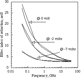 Fig. 4: Measured (solid
lines) and modeled results (dashed lines) for the effective index of refraction
[[beta]]/[[beta]]o (slow wave factor) at 0 V, 2 V reverse bias on center
conductor, and 7 V reverse bias on center conductor.
Fig. 4: Measured (solid
lines) and modeled results (dashed lines) for the effective index of refraction
[[beta]]/[[beta]]o (slow wave factor) at 0 V, 2 V reverse bias on center
conductor, and 7 V reverse bias on center conductor.