Jaeheon Han and Dean P. Neikirk
Microelectronics Research Center and Department of Electrical and Computer Engineering,
The University of Texas at Austin
Please see our full paper on this work:
J. Han and D. P. Neikirk, "Deflection behavior of Fabry-Perot pressure sensors having planar and corrugated membrane," SPIE's Micromachining and Microfabrication '96 Symposium: Micromachined Devices and Components II, R. Roop and K. Chau, Proc. SPIE 2882, Austin, Texas, USA, 14-15 October, 1996, pp. 79-90.
The following is a condensed version of the paper referenced above.
Slides used in our talk at this conference (file is about about 200 K).
Also refer to our other work on these Fabry-Perot Based Pressure Transducers .
This file created: Feb. 4, 1997
ABSTRACT
Micromachined Fabry-Perot microcavity structures have been investigated for use as pressure sensors. For the application of pressure sensors, the devices are categorized based on the shape and location of the deflecting diaphragm. Discussed here are planar bottom, planar top, and corrugated top diaphragm Fabry-Perot microcavity structures. Output signal degradation as a function of pressure, referred to as the signal averaging effect, caused by the non-planar deflection of an edge-clamped diaphragm, is reduced using planar top diaphragm structures, as compared to planar bottom diaphragm structures. This is achieved by improving the flatness of the deflecting diaphragm in the optically sampled area of the planar top diaphragm structures by adjusting the ratio of the top diaphragm area to the bottom diaphragm area. Corrugation of the top diaphragm structure further enhances flat deflection. However, the corrugated structures induce a static deflection of the diaphragm due to localized internal stress generated by the asymmetry of the corrugation on the diaphragm, referred to as the zero-pressure offset effect. The existence and influence of these parasitic effects have been observed using real-time measurements of the diaphragm deflection.
1. INTRODUCTION
Optical metrology is promising, but not extensively commercialized for sensor applications. Of the several optical techniques available, Fabry-Perot interferometry provides a high degree of sensitivity, versatility and immunity to environmental noise. Fabry-Perot based sensors have been broadly studied due to their capabilities for signal "amplification" (i.e., resonance) and tunability [1,2]. Fabry-Perot based devices such as pressure sensors and tunable filters have been built conventionally by using a hybrid two-wafer assembly technique that requires a fusion bonding process [3-5]. The fusion bonding process can limit the flexibility and the accuracy of the device structure dimensions, and restricts the compatibility with conventional VLSI fabrication technology. The surface micromachining method has recently emerged as a way to overcome the drawbacks of the hybrid assembly technique [6,7].
In this study, Fabry-Perot microcavity structures for use as pressure sensors are discussed, fabricated using a surface micromachined sacrificial layer process instead of a hybrid fusion bonding process [8]. This approach allows better device performance compared to hybrid fusion bonding through precise control of the cavity gap spacing, and higher manufacturing yield by enhancing the simplicity of fabrication and the compactness of the device [9].
The Fabry-Perot optical pressure sensor has recently been introduced as an alternative to conventional piezoresistive and capacitive pressure sensors to eliminate signal degradation in harsh environments. In addition piezoresistive pressure sensors show non-linear sensitivity at elevated temperature, and capacitive pressure sensors produce fairly small output capacitance. While a micromachined Fabry-Perot pressure sensor enjoys advantages over counterparts, its commercialization is still in early stage of maturity.
One of the major obstacles to commercialization is the degradation of device performance due to non-planar deflection of an edge clamped moving diaphragm [10]. Since it is impossible to build an unclamped, free-standing, deflecting diaphragm in the real world, the focus is to minimize the non-planarity of the deflection under applied external load. The first approach is to control the active device area, i.e., the "optically sampled area," by maximizing the ratio of the area of the deflecting diaphragm to the area of the stationary diaphragm. This will be accomplished by making the top diaphragm the deflecting diaphragm, rather than the bottom diaphragm as in previous work [10]. The second approach is to add corrugation to the deflecting diaphragm. The corrugation behaves like a spring or hinge. Both implementations are equally important to other sensing devices using clamped moving diaphragms, including the above mentioned piezoresistive and capacitive pressure sensors. For a piezoresistive pressure sensor, the deflecting diaphragm changes internal strain and, subsequently, the output resistance [11]. For a capacitive pressure sensor, the deflecting diaphragm, as an electrode of a capacitor structure, changes the electrode gap spacing and, subsequently, the output capacitance [12]. For both cases, non-planar deflection of a diaphragm deteriorates the linearity and the averaged magnitude of output signal. In the case of the Fabry-Perot optical pressure sensors, the deflection behavior of a diaphragm and its resulting device characteristics are presented by adapting and comparing the different deflecting diaphragm schemes, such as planar bottom diaphragm, planar top diaphragm, and corrugated top diaphragm.
2. DEVICE FABRICATION
Fabricated Fabry-Perot pressure sensors are classified into three types based on the location and the shape of a deflecting diaphragm. These are planar bottom diaphragm pressure sensor, planar top diaphragm pressure sensor, and corrugated top diaphragm pressure sensor.
2.1 Process for a planar bottom diaphragm pressure sensor
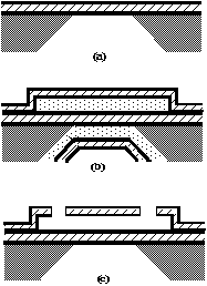
Figure 1 schematically illustrates the fabrication procedure for a planar bottom diaphragm pressure sensor [13]. Lightly doped 4-inch single crystal (100) silicon wafers are used as a substrate. The wafers are double-side polished and 300 um thick. The 0.7 um thick air gap is created when the sacrificial polysilicon embedded between two diaphragms is removed.
Each diaphragm consists of a multiple film stack of two silicon nitride layers cladding a silicon dioxide layer. These dielectric films are deposited using Low Pressure Chemical Vapor Deposition (LPCVD). The thickness of each layer is chosen in such a way that the Fabry-Perot microcavity is mechanically stable, i.e., it should not buckle or crack, and must have optimal characteristics of the optical response [7,14,15]. The total residual stress of the stack should be weak tensile to allow the diaphragm to remain flat when it is released during the sacrificial polysilicon etch step. Taking both the mechanical stability and the optical response into account, two 750 Å thick silicon nitride layers cladding a 4500 Å thick silicon dioxide layer are used for the top diaphragm, and two 1500 Å thick silicon nitride layers cladding a 10500 Å thick silicon dioxide layer are used for the bottom diaphragm. Silicon nitride is deposited by reaction of ammonia (NH3) and dichlorosilane (SiCl2H2) at a gas flow rate of 3.5:1 at 800 C and 220 mTorr. Silicon dioxide is deposited by reaction of silane (SiH4) and oxygen (O2) at a gas flow rate of 3:4 at 450 C and 110 mTorr.
The first step is to deposit the multiple film stack as a bottom diaphragm. After depositing the bottom diaphragm layers directly on the substrate, the dielectric film stack on the back side of the double-side polished wafer is patterned and plasma etched. The plasma etching of the silicon dioxide and silicon nitride stack is performed using CF4 and O2. The remaining back-side dielectric film stack becomes a masking layer for the subsequent wet KOH silicon anisotropic etching. The silicon substrate is anisotropically etched using 40% KOH solution at 80 C.
After forming the bottom diaphragm on the front side of the wafer, a 0.7 um thick LPCVD undoped polysilicon layer is deposited at 650[ring] C using silane (SiH4), and then patterned using 25 HNO3 : 13 H2O : 1 HF (by volume) having an etch rate of 6000 Å/min. The sacrificial polysilicon layer determines the gap spacing and the lateral size of the Fabry-Perot microcavity.
The next step is to deposit the top diaphragm dielectric layers over the patterned polysilicon. After the deposition of the top diaphragm, the etch windows are directly patterned on the top diaphragm to allow access to the sacrificial polysilicon layers encapsulated by the top and the bottom diaphragms. Plasma etching is performed to define the windows. The polysilicon is then etched using KOH. Both the top and the bottom diaphragms are freed to form the Fabry-Perot microcavity structure after etching the sacrificial layer. To avoid sticking problems, the wafer is rinsed 20 minutes first in de ionized (DI) water and then 20 minutes in isopropyl alcohol, before being dried. This final rinse with a low surface tension liquid helps prevent sticking problems.
Figure 1. Schematic view of fabrication procedure for planar bottom diaphragm pressure sensor; (a) formation of bottom diaphragm; (b) patterning and deposition of polysilicon and top diaphragm; (c) etch window formation and sacrificial polysilicon etching.
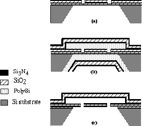
Figure 2. Schematic view of fabrication procedure for planar top diaphragm pressure sensor; (a) formation of bottom diaphragm and etch windows; (b) patterning and deposition of polysilicon and top diaphragm; (c) blanket backside and sacrificial polysilicon etching.
2.2 Process for planar and corrugated top diaphragm pressure sensors
One drawback of the planar bottom diaphragm pressure sensor is degradation of output signal intensity as a function of pressure caused by variation in the amount of deflection over the optically sampled area. The optically sampled area, which is the active device area, is mainly defined by the bottom diaphragm, since the bottom diaphragm should be smaller than the top diaphragm. Under the configuration of a Fabry-Perot pressure sensor with a deflecting bottom diaphragm, there are no means to reduce the parasitic output signal degradation effect because the entire area of the bottom diaphragm is within the optically sampled area. The maximum size of a bottom diaphragm is also limited by the size of the top diaphragm that is more fragile due to the relatively weak edge clamping mechanism and the existence of stress concentrators such as etch windows. This limitation of a Fabry-Perot pressure sensor with a deflecting bottom diaphragm deteriorates device performance and impedes further improvement.
The Fabry-Perot pressure sensor having a top diaphragm as the deflecting diaphragm reduces the limitations mentioned above. Figure 2 illustrates the fabrication process flow of a planar top diaphragm pressure sensor. The major obstacle to building the planar top diaphragm pressure sensors is implementing the etch windows on the bottom diaphragm without causing any discontinuity or void during the subsequent deposition process steps, such as polysilicon and top diaphragm multilayer dielectric deposition. This can be resolved by introducing sacrificial dielectric layers before depositing the bottom diaphragm layers.
The first step of fabrication is to deposit the sacrificial dielectric layers: a 300 Å thick silicon nitride and 5000 Å thick silicon dioxide stack. These are deposited using LPCVD. The 5000 Å silicon dioxide is the main sacrificial layer. The thin 300 Å silicon nitride is the barrier layer to protect the main sacrificial layer from overetching damage of the KOH wet anisotropic silicon substrate etching step.
The bottom diaphragm dielectric stack is then deposited directly on top of the sacrificial dielectric layers. The bottom diaphragm consists of two 750 Å thick silicon nitride layers cladding a 4500 Å thick silicon dioxide layer, all deposited using LPCVD. Next, the dielectric layers on the back side of the double-side polished wafer are patterned and plasma etched. Using patterned back side layers as a mask, the silicon substrate is anisotropically etched with 40% KOH solution at 80[ring] C to form the square dielectric bottom diaphragm on the front side of the wafer. At this stage, the defined bottom diaphragm is the combined dielectric stack of both sacrificial and bottom diaphragm layers.
The next step is to form etch windows in the bottom diaphragm using plasma etching from the front side of the wafer. The etch windows will later allow access to the sacrificial polysilicon layer that must be removed in the final stage of the fabrication to form the air gap between top and bottom diaphragm. The etching should stop at approximately half the thickness of the sacrificial silicon dioxide layer after the complete removal of the bottom diaphragm dielectric layers inside the patterned etch window area. This will prevent any void or discontinuity during the subsequent deposition layers in the etch window since the bottom diaphragm is still "continuous" due to the remaining sacrificial dielectric layer.
A 0.7 um thick LPCVD sacrificial polysilicon layer is next deposited to set the gap between the diaphragms of the final Fabry-Perot microcavity. This is followed by overcoating the patterned polysilicon with another dielectric stack. This dielectric stack, two 1500 Å thick silicon nitride layers cladding a 10500 Å thick silicon dioxide layer, forms the top diaphragm and is freed after etching the polysilicon.
After depositing the top diaphragm layers, all layers stacked on the back side of the wafer, including the sacrificial dielectric silicon dioxide and nitride layers, are removed by multiple blanket wet and plasma etching steps. Then, the sacrificial polysilicon is exposed through the etch windows from the backside of the bottom diaphragm. The polysilicon is etched using a KOH solution. Both the top and the bottom diaphragms are thus released to form the Fabry-Perot microcavity structure.
Corrugated top diaphragm pressure sensor are fabricated using the planar top diaphragm pressure sensor process flow but with an additional corrugation masking step after patterning the undoped LPCVD polysilicon. The corrugation depth of 0.35 um is half of the air gap spacing in thickness. The deposited top diaphragm dielectric film stack on the corrugation-etched polysilicon layer replicates profile underneath. Figure 3 shows the schematic cross-sections and the optical microscopic top views of a planar and a corrugated top diaphragm pressure sensor.
(a) Planar device (b) Corrugated device
Figure 3. Schematic cross-sections and optical microscopic top views of a planar and a corrugated top diaphragm pressure sensor.
3. MEASUREMENT RESULTS
3.1 Measurement set-up
A 2x2 optical fiber directional coupler is interconnected to the device, that is placed in the sealed sample chamber. The chamber is connected to compressed dry air and a calibrated pressure gauge. A 633 nm He-Ne laser is focused at one of the input ports of the directional coupler, and the reflected intensity is measured from the other of the input ports. One of the output ports is aligned to the device through the sealed, pressurized sample chamber. The transmitted intensity is obtained by placing the photodetector directly after the sample chamber. The other of the output ports is placed in index matching liquid to avoid reflections from the end of the unused port of the directional coupler. The optical fiber used was a 100 um diameter core / 145 um diameter clad multi-mode fiber.
When there is no optical fiber connection, the device located inside the sealed sample holder is placed between the beam splitter (or the collimator) and the photodetector. The measured transmittance is obtained by comparing the Fabry-Perot microcavity and a pinhole both having the same size. The measured transmitted and reflected data with the optical fiber setup is compared to those with free space setup (without optical fiber) to check the consistency of the measured results.
3.2 Optical response of planar diaphragm pressure sensors
The measured optical response can be compared to a simple model of the optical response of the Fabry-Perot cavity. Figure 5 shows the measured and the calculated transmitted intensities of the Fabry-Perot pressure sensors with a deflecting top diaphragm 300 um in diameter. The calculated transmitted intensities are obtained from the Fabry-Perot interference formula found by assuming normal incidence of light, negligible absorptance, and plane wave condition [7,16].
The measured transmitted intensities are in good agreement with the calculated ones. Degradation of the measured intensity over the calculated intensity with increasing applied pressure shows the signal averaging effect on the optical response. The signal averaging effect, which is the pressure dependent degradation of the output optical response, is caused by the variation in the amount of the deflection over the optically sampled area due to the bowing nature of the deflecting diaphragm.
The parasitic signal averaging effect can be reduced by enhancing the flatness of the diaphragm deflection within the optically sampled area by controlling the ratio of the area of the top diaphragm to the area of the bottom diaphragm. Figures 5 and 6 show that the pressure dependent behavior of the measured transmitted light intensities of the device having a top and bottom diaphragm with diameters of 300 um and 110 um, respectively, shows less degradation than that of the device having a top and bottom diaphragm with diameters of 300 um and 200 um, respectively.
The signal averaging effect is much more dramatic when we compare planar bottom and planar top diaphragm pressure sensors. Figure 7 shows the pressure dependent variation of the reflected intensity for the planar top and the planar bottom diaphragm Fabry-Perot pressure sensors. The deflecting diaphragms of both devices have the same size (150 um) and the same composite layer thicknesses (1500 Å Si3N4/10500 Å SiO2/1500 Å Si3N4). As expected from the above results, the deflecting top diaphragm device shows significantly less pressure-dependent degradation of the reflected light intensity behavior than the deflecting bottom diaphragm device.
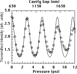
Figure 5. Measured transmitted intensity as a function of pressure for a planar top diaphragm Fabry-Perot pressure sensor with 300 um diameter circular top diaphragm and 110 um length square bottom diaphragm (dots: measured data; line: calculated).
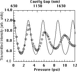
Figure 6. Measured transmitted intensity as a function of pressure for a planar top diaphragm Fabry-Perot pressure sensor with 300 um diameter circular top diaphragm and 200 um length square bottom diaphragm (dots: measured data; line: calculated).
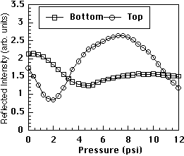
Figure 7. Measured reflected intensity as a function of pressure for a planar top and planar bottom diaphragm Fabry-Perot pressure sensor.
The improvement in device performance of the deflecting top diaphragm device compared to the bottom deflecting diaphragm device can be explained as follows: for the planar bottom diaphragm device the entire area of the deflecting, edge-clamped bottom diaphragm is included within the optically sampled area, while for the top diaphragm device the optically sampled area is only a small portion of the entire area of the deflecting top diaphragm. By making the ratio of the area of the top diaphragm to the area of the bottom diaphragm as large as possible while having a detectable output optical response, the parasitic signal averaging effect is minimized in the planar top diaphragm pressure sensor. This can make the top diaphragm device more desirable despite its increased process complexity.
A thick, small diaphragm can be used for maximum stiffness to increase the linear region of optical response as a function of pressure. The linear region of the optical response corresponds to movement within about a quarter of a wavelength of the incoming light source (about half a peak-to-peak cycle period). In our case, with the HeNe laser, it will be about 158 nm. The linear region becomes larger with a thicker and smaller deflecting top diaphragm.
3.3 Optical response of corrugated diaphragm pressure sensors
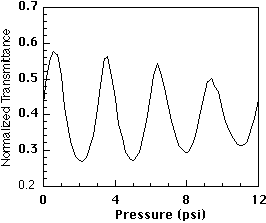
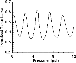
Corrugation was implemented on the planar top diaphragm Fabry-Perot microcavity structure to achieve further improvement in device characteristics, especially further reduction of the parasitic signal averaging effect by enhancing the flatness of the deflected diaphragm with applied pressure. Figure 9 shows the pressure dependent transmittance behavior of the planar and the corrugated device for a 300 um diameter top diaphragm. The corrugated device has a single 30 um width corrugation ring placed at the outside of the optically sampled area in the top diaphragm.
For the planar top diaphragm device, the signal averaging effect on the optical response prevails as the applied pressure increases. The averaging effect, that is, the pressure dependent degradation of output optical response, causes degradation of the output optical response with the applied pressure. However, for the corrugated top diaphragm device, the amplitude of transmittance increases steadily with applied pressure until it reaches a maximum, then decreases with further increase of applied pressure. This indicates that at zero pressure the corrugated top diaphragm is already deflected, concave in our case, due to the non-uniformly distributed out-of-plane internal stress induced by the asymmetry of the corrugation structure with respect to the horizontal plane of the diaphragm.
(a)
(b)
Figure 9. The measured transmittance as a function of the Fabry-Perot pressure sensor with a 300 um diameter (a) planar and (b) corrugated top diaphragm.
This nonplanar, localized stress-induced deflection of a diaphragm without external load is called "zero pressure offset" [17-19]. The zero pressure offset phenomenon had been previously suggested through simulation work using the finite element method [15, 20].
4. REAL-TIME THREE-DIMENSIONAL ANALYSIS OF DEFLECTION BEHAVIOR
A real-time three dimensional image was obtained with a Lasertech confocal scanning laser microscope by scanning and integrating the planar image, while varying the focal plane. This is then done as a function of applied pressure. The resolution in vertical direction depends on the scan range. For higher magnification, the scan range is smaller and the resolution is higher at the expense of the total sampling area.
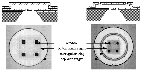
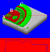
Figures 10 shows results and three-dimensional images obtained from the confocal microscope for Fabry-Perot pressure sensors having 150 um diameter top diaphragm with a 15 um width corrugation ring. The positions A and C are the center and the edge location of the top diaphragm, respectively. The position B is the middle location for the planar top diaphragm or the inner edge location in front of the corrugation ring for the corrugated top diaphragm. For the corrugated devices, the zero pressure offset effect is initially dominant where the diaphragm is concave in shape, and then with applied pressure a planar shape is produced throughout the entire inner portion. As shown at 20 psi in Figure 10 (c), respectively, the active inner portion of the diaphragm maintains its planarity, while the profile of the corrugated area changes. The observed pressure dependent variations of the shape of the deflecting diaphragm with or without the corrugation are in good agreement with the characteristics of the measured optical responses.
 (a)
(a)
 (b) 0 psi
 (c) 20 psi
Figure 14. Three-dimensional confocal laser scanning microscope images as a function of pressure for a 150 um diameter corrugated top diaphragm Fabry-Perot pressure sensor: (a) plot of deflection versus position and pressure; (b) 0 psi three-D image; (c) 20 psi three-D image.
5. DISCUSSION AND CONCLUSIONS
Micromachined Fabry-Perot interference based microcavity structures have been studied for use as pressure sensors. The fabricated pressure sensors are classified into three categories depending upon the shape and the location of the deflecting and sealed diaphragm. These are the planar bottom diaphragm pressure sensor, the planar top diaphragm pressure sensor, and the corrugated top diaphragm pressure sensor. The composite dielectric layers of the diaphragms have been optimized for proper mechanical stability and output optical response.
Fabrication complexity and device characteristics of these pressure sensors have been compared to one another. Planar bottom diaphragm pressure sensors are the easiest to build, but their device characteristics are limited. On the other hand, corrugated top diaphragm pressure sensors are the most complicated to build, but can provide more design flexibility. Performance distinctions include differences in two parasitic phenomena: the signal averaging effect and the zero pressure offset effect. Both phenomena are due to the non-planar bending behavior of an edge clamped diaphragm.
The signal averaging effect is the pressure dependent degradation of output optical responses due to the bowing nature of the edge-clamped diaphragm under applied external load. The increased deviation of the measured and the calculated transmitted intensities as a function of pressure, e.g., the damping of the measured response, indicates this effect. Significant enhancement of device performance from the planar top diaphragm pressure sensors over planar bottom diaphragm pressure sensors is achieved by reducing the parasitic signal averaging effect by adjusting the optically sampled area.
Another way to enhance the flatness of the deflecting diaphragm is to add a corrugation structure to the planar diaphragm. However, this approach causes static deflection of a diaphragm without applied pressure, called the zero pressure offset effect. This is due to the non-uniformly distributed out-of-plane internal stress produced by the asymmetry of the localized corrugated structure with respect to the horizontal plane of the diaphragm. This is the first experimental demonstration of this effect in a Fabry-Perot microcavity structure.
6. ACKNOWLEDGMENTS
This work was sponsored by the Advanced Research Projects Agency (ARPA) Embedded Microsystems Program under contract # DABT63-92-C-0027 AMD P00002- DOD-ARPA.
7. REFERENCES
1. J. P. Dakin, C. A. Wade, and P. B. Withers, "An Optical Fiber Pressure Sensor," SPIE Fiber Optics '87: Fifth International Conference on Fiber Optics and Optoelectronics, vol. 734, pp. 194-201, 1987.
2. J. Farah, "Interferometric Fiber Optic Displacement Sensor," 1995, USA, Patent # 5420688.
3. B. Halg, "A silicon pressure sensor with a low-cost contactless interferometric optical readout," Sensors and Actuators A, vol. 30, pp. 225-229, 1992.
4. J. H. Jerman, D. J. Clift, and S. R. Mallinson, "A Miniature Fabry-Perot Interferometer with a Corrugated Silicon Diaphragm Support," Tech. Digest IEEE Solid-State Sensor and Actuator Workshop, pp. 140-144, 1990.
5. M. A. Chan, S. D. Collins, and R. L. Smith, "A Micromachined Pressure Sensor with Fiber-optic Interferometric Readout," Sensors and Actuator, vol. 43, pp. 196-201, 1994.
6. P. M. Sarro, A. W. Herwaarden, and W. Vlist, "A Silicon-silicon nitride Membrane Fabrication Process for Smart Thermal Sensors," Sensors and Actuators A, vol. 41-42, pp. 666-671, 1994.
7. K. Aratani, P. J. French, P. M. Sarro, D. Poenar, R. F. Wolffenbuttel, and S. Middlehoek, "Surface Micromachined Tunable Interferometer Array," Sensors and Actuators, vol. A 43, pp. 17-23, 1994.
8. Y. Kim and D. P. Neikirk, "Micromachined Fabry-Perot Cavity Pressure Transducer," IEEE Photonics Technology Letters, vol. 7, pp. 1471-1473, 1995.
9. Y. Kim and D. P. Neikirk, "Design for Manufacture of Micro Fabry-Perot Cavity-based Sensors," Sensors and Actuators A, vol. SNA050/1-2, pp. 141-146, 1995.
10. Y. Kim, "Application of Micromachining Techniques for Fabry-Perot cavity Based Microsensors," 1995, Ph D Dissertation, The University of Texas at Austin.
11. K. Suzuki, T. Ishihara, M. Hirata, and H. Tanigawa, "Nonlinear Analysis on CMOS Integrated Silicon Pressure Sensor," IEEE International Electron Devices Meeting, Washington, DC, 137-140, December, 1985.
12. C. Sanders, J. Knutti, and J. Meindl, "A Monolithic Capacitive Pressure Sensor with Pulse-Period Output," IEEE Transactions on Electron Devices, vol. ED-27, pp. 927-930, 1980.
13. Y. Kim and D. P. Neikirk, "Micromachined Fabry-Perot Cavity Pressure Transducer with Optical Fiber Interconnects," Micromached Devices and Components, R. Roop and K. Chau ed., Austin, Texas, USA, 242-249, 23-24 October, 1995.
14. R. Schellin, G. Hess, W. Kuhnel, C. Thielemann, D. Trost, J. Wacker, and R. Ssteinmann, "Measurements of the Mechanical Behavior of Micromachined Silicon and Silicon-nitride Membranes for Microphones, Pressure Sensors, and Gas Flow Meters," Sensors and Actuators A, vol. 41-42, pp. 287-292, 1994.
15. S. T. Cho, K. Najafi, and K. D. Wise, "Internal Stress Compensation and Scaling in Ultrasensitive Silicon Pressure Sensors," IEEE Trans. Electron Devices, vol. ED-39, pp. 836-842, 1992.
16. J. H. Jerman, D. J. Clift, and S. R. Mallinson, "A Miniature Fabry-Perot Interferometer with a Corrugated Silicon Diaphragm Support," Sensors and Actuators A, vol. 29, pp. 151-158, 1991.
17. P. R. Scheeper, W. Olthuis, and P. Bergveld, "The Design, Fabrication, and Testing of Corrugated Silicon Nitride Diaphragms," J. of Microelectromechanical Systems, vol. 3, pp. 36-42, 1994.
18. Y. Zhang and K. D. Wise, "Performance of Non-planar Silicon Diaphragms under Large Deflections," J. of Microelectromechanical Systems, vol. 3, pp. 59-68, 1994.
19. Y. Zhang and K. Wise, "Performance of Silicon Diaphragms under Large Deflections," IEEE Micro Electromechanical Systems Workshop, Fort Lauderdale, FL, 284-288, Feb., 1993.
20. Y. Zhang, S. Crary, and K. Wise, "Pressure Sensor Design and Simulation using the CAEMEMS-D Module," IEEE Solid-State Sensor and Actuator Workshop, Hilton Head, SC, 32-35, June, 1990.