A Comparison of MIS Slab and Pillar Microstrip Lines for use as Digital Interconnects
Emre Tuncer, Dean P. Neikirk, and Lawrence T. Pillage
Department of Electrical and Computer Engineering
The University of Texas at Austin
Austin, TX 78712
Abstract
Time domain pulse propagation has been considered on both conventional ("slab") MIS (Metal-Insulator-Silicon) and etched "pillar" MIS microstrip lines as a function of silicon substrate resistivity. Accurate quasi-static calculations have been used to compare the performance of the pillar and normal MIS lines for substrate resistivities of 1000 ohm-cm, 10 ohm-cm, and 0.1 ohm-cm, using series termination to achieve optimum waveform shape.
Summary
For the last two decades the speed of digital circuits has increased considerably. In order to achieve higher speeds, high chip-packing density is desired; Multi-Chip Modules (MCM's) are being widely considered for this purpose. The interconnect structures on MCM's are usually microstrips over insulating substrates. Due to its availability and low cost, it may be advantageous to fabricate the interconnects directly on a semiconducting silicon substrate. In the case of silicon, propagation delays may be higher due to both the high relative dielectric constant, and the possibility of slow wave effects. A way of shortening delay and decreasing loss may be to remove unnecessary silicon in the substrate, as shown in Figure 1.
In this study, the propagation characteristics of an interconnect on an Si-SiO2 pillar are investigated and compared to that of a conventional (slab) MIS microstrip [1]. For the microstrip, the propagation constant is obtained from the series impedance per unit length Z and shunt admittance per unit length Y which are calculated by applying transverse resonance and quasi-static analysis [2]. The same approach is used for the pillar but the equivalent circuits are modified so that the substrate material which is removed is treated appropriately. This approach has been shown to agree with full wave results over a very wide range of frequency and substrate conductivity [2].
For the purposes of the simulations, the metal strip is taken to be 1
um thick and 10 um wide. SiO2 layer and Si substrate are 1 um and 500 um
thick, respectively. The propagation constant is calculated for three values
of substrate resistivity, 0.1 ohm-cm, 10 ohm-cm, and 1000 ohm-cm. Figure
2 illustrates the dependence of neff ([[beta]]/[[beta]]o) on the
substrate resistivity for the slab. All curves have the same value for low
frequency, since at low frequency the interconnect is an RC line, with capacitance
given by the capacitance across the SiO2 layer and resistance given by the
dc metal resistance. At about 2 x 10⁸ Hz (Rdc/2[[pi]]L),
the line becomes RLC, and assumes the usual slow-wave behavior. When the
frequency exceeds the dielectric relaxation frequency the lines operate
in the quasi-dielectric mode, and neff compares well with established
values [3]. In Figure 3, the same curves for the pillar structure are shown.
The high frequency value of neff is smaller than that of slab since
the capacitance of the strip is smaller because some of the high dielectric
material has been removed. The effective dielectric relaxation frequencies
are also lower, because the capacitance and conductance are no longer related
to each other by the constant [[epsilon]]/[[sigma]]. The conductance is
smaller than of that the slab, so the effective dielectric frequency is
smaller than the bulk value for the substrate. Figures 4 and 5 show the
attenuation constants for the same cases. For low frequency the loss mechanism
is due to the RC line behavior. For the pillar, 1000 ohm-cm case has the
lowest loss because loss is proportional to ![]() and capacitance
is decreasing due to the transition to the quasi-dielectric mode. The slab
has higher loss for the same resistivity, because there is more lossy material
in the path of electric fields. For the 10 ohm-cm case, loss in the slab
is much higher than to that of the pillar. For the slab the slow-wave quasi-dielectric
transition occurs at a higher frequency, thus increasing loss. For the 0.1
ohm-cm case, before the quasi-dielectric mode occurs, the skin-effect mode
occurs, since the skin-depth in the substrate is equal to the thickness
at 6.4 GHz. After this point, currents would flow in the substrate; for
the pillar there is less material to carry these currents, giving higher
loss than the slab.
and capacitance
is decreasing due to the transition to the quasi-dielectric mode. The slab
has higher loss for the same resistivity, because there is more lossy material
in the path of electric fields. For the 10 ohm-cm case, loss in the slab
is much higher than to that of the pillar. For the slab the slow-wave quasi-dielectric
transition occurs at a higher frequency, thus increasing loss. For the 0.1
ohm-cm case, before the quasi-dielectric mode occurs, the skin-effect mode
occurs, since the skin-depth in the substrate is equal to the thickness
at 6.4 GHz. After this point, currents would flow in the substrate; for
the pillar there is less material to carry these currents, giving higher
loss than the slab.
To see the effects of the different lines on pulse propagation we consider a line 5 cm long. A 100 MHz clock (pulse repetition rate) is applied to the input with a rise time of 0.1 ns. For this rise time, frequencies from dc up to about 20 GHz are important. In the example, the line is terminated with a 10 fF capacitor at the output. A series termination (Rs) is also used to damp reflection-induced oscillations; the series termination also determines overshoot of the pulse at the output. By selecting the correct value, overshoot and ringing at the output can be reduced, while maintaining a fast rise-time. For low-loss lines, the high frequency impedance of the line is usually the optimum series termination value. However, when the loss is high, self-termination effects are important, and the optimum series termination value decreases.
In Figures 6 and 7, the output waveforms are plotted for the pillar and slab for a substrate resistivity of 1000 ohm-cm for different values of Rs. The delay in the pillar is much shorter, and it is less lossy. The optimum value of series termination is thus higher for the pillar. At this clock speed, the slab waveform never goes to zero, but for the optimum value of series termination, the pillar waveform has a clear pulse shape from 0 to 1 V. At 10 ohm-cm, Figure 8 illustrates the fact that the pillar is self-terminating. In this case, the slab is less lossy than the pillar; however, the pillar is much faster than slab. As the resistivity drops to 0.1 ohm-cm, in the frequency range of interest, the wave in both of the structures is always slow. Figure 9 shows that for the 0.1 ohm-cm substrate the pillar and slab microstrips produce nearly identical pulse propagation characteristics. In conclusion, we have compared the behavior of both slab and pillar MIS microstrip lines, and have shown the trade-offs between delay time, series termination resistance, and silicon substrate resistivity.
References
1. H. Hasegawa, M. Furukawa, and H. Yanai, "Properties of microstrip line on Si-Si02 system," IEEE Trans. Microwave Theory Tech., vol. MTT-19, pp. 869-881, Nov. 1971.
2. E. Tuncer and D. P. Neikirk, "Highly accurate quasi-static modeling of microstrip lines over lossy substrates," IEEE Microwave and Guided Wave Letters, vol. 2, pp. 409-411, Oct. 1992.
3. K. C. Gupta, R. Garg, and I. J. Bahl, Microstrip Lines and Slotlines, Norwood: Artech, 1979, ch. 1.
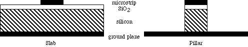
Figure 1: Geometry of normal (slab) and pillar MIS microstrips. For the pillar, all silicon is removed except that directly under the metal interconnect line. In the calculations discussed here, the pillar is surrounded by air ([[epsilon]]r = 1).
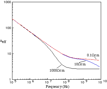
Figure 2 : neff ([[beta]]/[[beta]]o) of MIS slab microstrip.
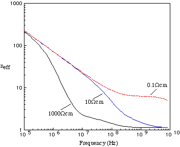
Figure 3 : neff ([[beta]]/[[beta]]o) of MIS pillar microstrip.
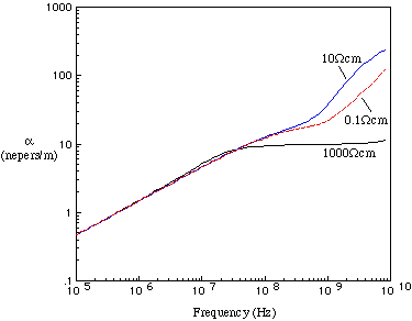
Figure 4 : Attenuation constant [[alpha]] of MIS slab microstrip.
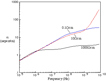
Figure 5 : Attenuation constant [[alpha]] of MIS pillar microstrip.
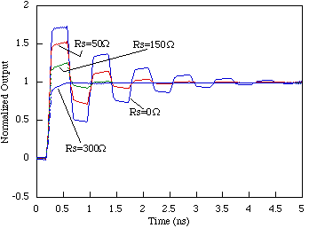
Figure 6 : Pulse propagation on MIS pillar, 1000 ohm-cm substrate resistivity. RS is the series termination resistance
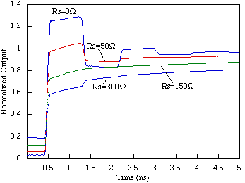
Figure 7 : Pulse propagation on MIS slab, 1000 ohm-cm substrate resistivity.
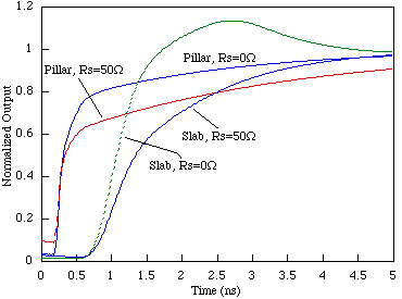
Figure 8 : Pulse propagation on MIS pillar and slab , 10 ohm-cm substrate resistivity.
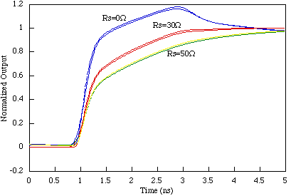
Figure 9 : Pulse propagation on MIS pillar and slab , 0.1 ohm-cm substrate resistivity; pillar and slab waveforms are virtually identical.