 (a)
(a) 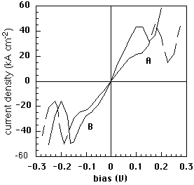 (b)
(b)K. K. Gullapalli and D. P. Neikirk
Microelectronics Research Center
The University of Texas at Austin, Austin, TX 78712 (512)-471-8104
A more complete discussion of this material can be found in our publications:
GaAs/AlAs tunneling diodes with N-N+-N buffer layers exhibit two stable I-V curves that remain distinct across zero bias.[1] Such devices can be repetitively switched between the curves by the application of an appropriate threshold voltage. Experimentally, the device maintains memory of its state even under short circuit conditions and for an indefinite duration. Previously, multiple steady state I-V curves in such diodes have been simulated using a quantum transport model based on the Wigner function.[2] Here, using a time-dependent Wigner-Poisson simulation, we show that transitions between the multiple curves can be produced by voltage transients in a manner very similar to that seen in experiment.
For the simulation we consider a double barrier quantum well structure consisting of an 18 monolayer (ML) lightly doped N-type (1015 cm-3) GaAs quantum well sandwiched between symmetric 6 ML lightly doped AlAs barriers. The quantum well structure is surrounded on both sides by an 18 ML N-type (1015 cm-3) GaAs layer, 36 ML N+ (4x1018cm-3) GaAs layer, and 36 ML N (1015 cm-3) GaAs layer. Finally, the device is embedded between thick N+ contact layers (4x1018cm-3 on the left side, 5x1018cm-3 on the right).
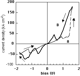
As a check on the simulation, the measured and calculated room temperature steady state I-V characteristics of the diode are qualitatively similar. The two solutions obtained produce different effective barriers to electron flow, producing distinct differential resistances even at zero bias. The electron density in the high impedance state is peaked in left N+ layer, whereas in the low impedance state there is a depletion of electrons in the left N+ layer.
The simulation of the switching transients shows behavior similar to the experimental switching cycle. With the device initially in the low impedance state, a -0.8 V bias was applied to right contact (left contact assumed as the reference). This causes the notch in the potential in the left N+ layer to be filled by the left contact, and in about 1 psec the time dependent simulation is now identical to the steady state solution at the same bias for the high impedance state. Thus, as in the experiment, the negative voltage step has induced "switching" from the low impedance to the high impedance state. Next, the voltage is stepped back to zero; the device remains in the high impedance state. The transient current does require a relatively longer time, about 4 psec, to reach its steady state value (zero, in this case). A voltage step of +0.8 V was then applied, causing the left N+ notch to deplete, and in about 1 psec the time dependent simulation becomes identical to the steady state solution for the low impedance state. Thus, again as in the experiments, the positive voltage step has induced "switching" from the high to the low state. We finish the simulations by stepping the voltage back to zero; in about 1 psec the transient current has decayed to zero, and the device remains in the low impedance state. In both the simulations and experiment, once in the low state, for positive bias transients the device remains in the low state; similarly, once in the high state, for negative bias transients the device remains in the high state.
[1] K. K. Gullapalli, A. J. Tsao and D. P. Neikirk, Appl. Phys. Lett. 62, 2856 (1993)
[2] K. K. Gullapalli, D. R. Miller and D. P. Neikirk, Phys. Rev. B 49, 2622 (1994)
(a) (b)
Figure 1: a) Measured and b) simulated room temperature I-V curves of multi-state quantum well diode. In the simulation, the spacer layers are narrower than in the experiment and hence the small voltages at which all the features appear.
 (a)
(a) 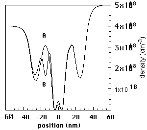 (b)
(b)
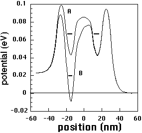
Figure 2: Calculated self-consistent potential and electron densities for the high impedance state (labeled A) and the low impedance state (labeled B) at zero bias.
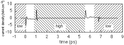
Figure 3: Simulated switching transient with the device initially in the low impedance state (A). As in experiment, a large negative voltage step (~-0.8V) causes a transition to the high impedance state. The low impedance state is recovered using a large (~0.8V) positive voltage step.