please see:
V. P. Kesan, D. P. Neikirk, B. G. Streetman, and P. A. Blakey, "A New
Transit Time Device Using Quantum Well Injection," IEEE Electron
Device Lett. EDL-8, April 1987, pp. 129-131.
V. P. Kesan, D. P. Neikirk, T. D. Linton, P. A. Blakey, and B. G. Streetman,
"Influence of Transit Time Effects on the Optimum Design and Maximum
Oscillation Frequency of Quantum Well Oscillators," IEEE Trans.
Electron Devices ED-35, April 1988, pp. 405-413.
Kiran Kumar Gullapalli, Master's thesis title: "Simulation of Electron
Transport in Double Barrier Diodes," The University of Texas at Austin,
1991.
Vijay Reddy, PhD dissertation title: "Characterization of High Frequency
Oscillators and Varactor Diodes Grown by Molecular Beam Epitaxy," The
University of Texas at Austin, 1994.
also see our work on experimental performance:
Experimental (Microwave
and DC) Operation of the Quantum Well Injection Transit Time (QWITT) Diode
Influence of Space Charge and Quantum
Well Negative Resistances on Resonant Tunneling Diodes
V.P. Kesan, D. R. Miller, V. K. Reddy, K. K. Gullapalli,
and D.P. Neikirk
Microelectronics Research Center, Department of Electrical and Computer
Engineering,
The University of Texas at Austin, Austin, Texas 78712.
ABSTRACT
This paper discusses the small-signal and linear analysis of resonant
tunneling diodes used as negative resistance oscillators. The analysis concentrates
on the transit (i.e., space charge) effects associated with a depleted spacer
layer outside the quantum well. Closed form expressions are derived for
small signal (linear) specific negative resistance based on the quantum
well current-voltage characteristics. Conditions under which transit effects
dominate device characteristics are shown to hold for most practical cases.
The analysis shows that the effective limit on the maximum oscillation frequency
of quantum well oscillators is determined largely by transit effects, rather
than the intrinsic characteristics of the quantum well.
Introduction
Tunneling through quantum wells has been the subject of much recent research
[1-14]. Because of the negative differential resistance exhibited by quantum
wells, and since tunneling is an inherently fast transport mechanism, these
devices have been proposed for use in extremely high frequency oscillators.
Encouraging preliminary experimental results for such oscillators have been
obtained at millimeter-wave frequencies [11, 13]. Experimentally, the quantum
well diode with the highest reported frequency of oscillation has required
the use of moderately doped spacer layers approximately 0.5 micron thick
on either side of the quantum well region [11, 13]. Such thick spacer layers
are expected to produce major effects on device performance, since a significant
portion of the spacer layer on the anode side of the quantum well may be
depleted, resulting in a transit-time delay. Deliberate exploitation of
transit-time effects in the anode side spacer layer should enhance the performance
of quantum well oscillators [22, 23], and such devices have been termed
quantum well injection transit (QWITT) diodes
[23]. In fact, the existence of significant depleted regions in the best
experimental quantum well oscillators suggests that these structures [11,
13] operate in a QWITT-mode. Small-signal analysis of the negative resistance
of transit-time diodes is useful for establishing oscillation thresholds,
and hence the structures needed to obtain the highest possible operating
frequencies from these devices. This paper presents such an analysis for
quantum wells with anode-side spacer layers (i.e. QWITT diodes), and presents
results which indicate the importance of transit/space charge effects for
device oscillation.
Small Signal Analysis
The physical structure under consideration is shown in Fig. 1(a). It
is assumed that the length of the quantum well region, l, is much
smaller than the depleted spacer layer length W. The depletion region transit-time
is thus much greater than the transit-time through the quantum well, and
so transport through the quantum well is considered to be instantaneous
here. The quantum well is treated as an injecting cathode whose small-signal
equivalent circuit is the 'cold' (geometric) capacitance of the well, in
parallel with a conductivity which represents the tunneling current (see
Fig. 1(b)). For small-signal analysis the quantum well is characterized
by a normalized injection conductance sigma, which is given by
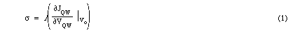
where JQW is the instantaneous current density, VQW
is the instantaneous voltage, and Vo is the dc bias voltage,
each across the quantum well region only, excluding the voltage dropped
across the depletion region. At present there are no generally accepted,
accurate theoretical models which predict the transport behavior (and hence
sigma) of quantum well structures. However, it is possible to estimate the
value of sigma using the dc J-V characteristics of quantum well diodes.
As noted above the terminal J-V characteristics must be corrected for any
voltage drops across depletion and contact regions. Examination of both
experimental and theoretical results [30-33] indicates that for a wide variety
of quantum well structures, when biased to produce negative differential
resistance, the room temperature value of sigma lies between about -0.05
ohm-1cm-1 and -0.5 ohm-1cm-1,
with an average value of about -0.3 ohm-1cm-1 . Note
that quantum well structures with large peak-to-valley ratios but lower
current density [30] have given lower values of sigma than that obtained
from structures with higher current density but lower peak-to-valley ratios
[11, 13, 32]. Thus, from a small-signal perspective, the magnitude of the
current density is more important than the peak-to-valley current ratio
for the quantum well. This large current density is related to the use of
thin quantum well barriers; in some cases [11,13] the barriers are more
than a factor of two thinner than other structures [30].

Figure 1: (a) Quantum well diode structure which exhibits significant transit-time
effects. The GaAs spacer layer on the cathode side of the quantum well region
is made thin to reduce parasitic series resistance. A thick, lightly GaAs
spacer layer is used on the anode side to produce a depletion region of
length W, much longer than the thickness of the quantum well region l.
. The transit-time through this layer is much larger than that through the
quantum well region, and space charge effects in this region of the device
can significantly affect the current-voltage curve; this device forms a
quantum well injection transit (QWITT) diode.
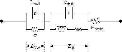
Figure 1: (b) Small-signal equivalent circuit for the structure shown in
(a). ZQW is the specific impedance,  ' is the effective dielectric
constant, and sigma is the injection conductance, of the quantum well; Ztt
is the specific impedance, and is the dielectric constant of the
depletion region. Rprstc represents the parasitic series resistance
due to any undepleted spacer regions, highly doped contact regions, and
ohmic contacts.
' is the effective dielectric
constant, and sigma is the injection conductance, of the quantum well; Ztt
is the specific impedance, and is the dielectric constant of the
depletion region. Rprstc represents the parasitic series resistance
due to any undepleted spacer regions, highly doped contact regions, and
ohmic contacts.
Once sigma has been found, the specific impedance of the quantum well injection
region at an angular frequency  is given by

where ' is the effective dielectric constant of the injection region. The
total small-signal specific impedance (excluding parasitic elements) of
the QWITT diode is the sum of this specific impedance and that of the depleted
spacer region Ztt

To obtain the specific impedance Ztt, charge transport through
the depleted (drift) region must be considered. Here it is assumed that
the depletion region electric field is high enough to cause injected charge
to traverse the depletion region at a constant saturated velocity vs. Although
this approximation will break down for extremely thin depletion regions
in which transient transport effects may be significant, it should be adequate
in establishing trends of device operation.
Use of a frequency-independent injection conductance sigma and a constant
saturation drift velocity permits the application of analytical methods
previously established for other transit-time devices [24-26]. Based on
these results, the specific impedance at an angular frequency for this device is
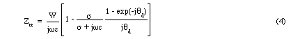
where is the dielectric constant of the drift region, and  is the drift
(or transit) angle, given by
is the drift
(or transit) angle, given by  . For simplicity the dielectric
constant of the quantum well region and the drift region have been assumed
to be equal in this case. The transit (space charge) specific negative resistance
that can be obtained from the depleted spacer region is the real part of
Eq. 4:
. For simplicity the dielectric
constant of the quantum well region and the drift region have been assumed
to be equal in this case. The transit (space charge) specific negative resistance
that can be obtained from the depleted spacer region is the real part of
Eq. 4:
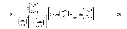
The specific resistance of the quantum well injection region given by the
real part of Eq. 2 is
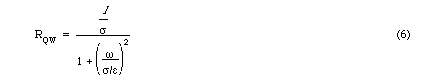
The total specific resistance of a QWITT diode (excluding parasitic resistance
in the device) is given by the sum of Eqs. 5 and 6. In conventional transit-time
devices the injection conductance is positive, yielding a positive injection
resistance, which must be overcome by a drift region negative resistance
to obtain oscillation. For a quantum well injection region sigma can be
negative, and thus the possibility of a negative injection conductance is
introduced. In such a case the resistance of both the transit-time region
and the injection region may be negative.
As expected from a transit-time analysis, there is a specific length of
the depletion region W which yields the maximum negative resistance for
any given frequency, injection conductance, and saturation velocity, given
by
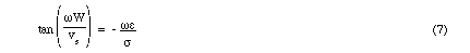
When using Eq. 7 it is necessary to select the appropriate branch of the
inverse tangent function. For sigma positive, Eq. 5 yields a negative resistance
only for the (2pi - pi/2, 2pi + pi/2) branch.
For sigma negative, the (-pi/2, pi/2) branch of the inverse tangent
function should be used. At any given frequency there is also an optimum
value of injection conductance sigma which will maximize the transit-time
negative resistance, given by

Substitution of Eq. 8 into Eq. 7 yields an optimum transit angle of 5pi/3
for positive sigma, and pi/3 for negative sigma. Thus, at a particular operating
frequency there is a unique combination of injection conductance sigma and
drift region length W that will yield the absolute maximum small-signal
transit-time negative resistance for this device, which is
 (9)
(9)
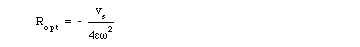
As noted above, the quantum well region can be biased so that it also
produces a negative resistance; this corresponds to the negative sigma case.
Considering Eq. 6 it is clear that there is a specific value of injection
conductance sigma which will maximize the negative resistance available
from the quantum well region, given by
 (10)
(10)
Comparing this to Eq. 8, it is found that quantum well negative resistance
is maximized at a value of |sigma| which is 31/2 larger than
that which maximizes the transit-time negative resistance. The relative
importance of the two regions to total negative resistance can be determined
by comparing the transit-time and quantum well negative resistances for
sigma chosen to maximize quantum well performance. Using Eqs. 6 and 10,
the maximum specific negative resistance available from the quantum well
region is
 (11)
(11)
For this value of sigma Eq. 7 yields an optimum transit angle of pi/2,
and Eq. 5 then gives the negative resistances available from the transit-time
region of the device as
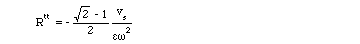 (12)
(12)
If transit time effects dominate the negative resistance of the device
then |Rtt| >> |RmaxQW,
which yields the condition
 (13)
(13)
Thus, at a given frequency, if the value of injection conductance is
chosen to maximize the quantum well negative resistance, transit time effects
will still dominate as long as the frequency is lower than 0.4vs/l.
Assuming a conservative saturation velocity of 6x106 cm/sec
and a typical quantum well length l of 10 nm, transit time effects
dominate when the operating frequency is less than approximately 380 GHz.
At this frequency a very high injection conductance of -2.7 (ohm-cm)-1
is required to satisfy Eq. 10.
If the value of injection conductance is fixed, rather than being allowed
to vary in accordance with Eq. 10, transit time effects may dominate over
an even wider frequency range than that indicated by Eq. 13. For a fixed
value of sigma, we should consider two limiting cases for Eqs. 5 and 6,
corresponding to <<  and >> . For low frequencies we have
 (14)
(14)
and
 (15)
(15)
The first term in Eq 15 is negative since sigma is negative. The second
term is always positive and represents the space-charge resistance familiar
in conventional transit-time device theory. The total Rd will
be negative if  . Thus, at low frequencies, the condition
to ensure that |Rtt| >> |RQW| is
. Thus, at low frequencies, the condition
to ensure that |Rtt| >> |RQW| is
 (16)
(16)
Using the typical values for vs and l given above,
Eq. 16 requires that |sigma| << 3.4 (ohm- cm)-
1, which is easily satisfied for the all quantum well structures studied
to date.
For high frequencies ( >> ), the limiting
values of negative resistance are given by
 (17)
(17)
and
 (18)
(18)
Thus, at high frequencies, the condition to ensure that |Rtt| >> |RQW|
is
 (19)
(19)
Again using typical values for vs and l , Eq. 19 leads
to the requirement that the operating frequency be less than 760 GHz.
Use of Eqs. 16 and 19 provides a more realistic constraint on the requirement
that |Rtt| >> |RQW| than Eq. 13, since
it appears very difficult to achieve values of |sigma| > 1 (ohm-cm)-1.
Hence, a sufficient condition to ensure that transit time effects dominate
the intrinsic quantum well negative resistance is that Eqs. 16 and 19 be
satisfied. For frequencies below , the QWITT diode exhibits a
constant, broad band negative resistance and for frequencies much greater
than , the resistance falls rapidly as -3.
Therefore, it is desirable to operate the device in the "low frequency"
regime where the negative resistance is constant and avoid the -3 falloff at frequencies much greater than . Figure 2 shows
the small signal negative resistance produced by a fixed injection conductance
of -0.4 (ohm-cm)-1, illustrating the relative contributions of
the quantum well and the depletion region, as well as their low and high
frequency behaviors.
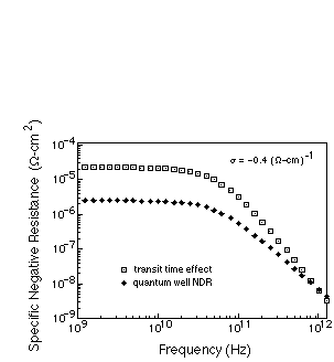
Figure 2: Small signal calculated negative resistance fro a QWITT diode
(from eqs. 5 and 6).
Small-signal analysis indicates that transit effects associated with the
anode side depleted spacer layer in quantum well oscillator/QWITT diodes
dominate design considerations. At any particular frequency of operation,
achieving maximum performance requires appropriate optimization of both
the depleted length of the anode spacer region and the quantum well injection
conductance. Appropriate optimization of these parameters is predicted to
yield QWITT devices whose RF performance potential is superior to that of
bare quantum wells. The structure of the best experimental quantum well
oscillators strongly suggests that they are in fact operating in a QWITT
mode; additional performance improvements should result from further systematic
optimization as suggested by the analysis presented in this paper.
QWITT Linear J - E Model
The QWITT diode was originally conceived as a "conventional"
transit-time device and the acronym stood for Quantum Well
Injection Transit-Time. The operation of transit-time
devices, in the conventional sense, usually requires that the phase delay
due to carrier transit-time in the drift region be a significant fraction
of the ac voltage cycle. For example, devices such as the impact-ionization
avalanche transit-time (IMPATT) diode operate only in a narrow frequency
band where the carrier transit-time is approximately half of the ac voltage
cycle (i.e., the drift angle, W/vsat, is pi). In
the QWITT diode when sigma > 0, the device exhibits narrow-band negative
resistance similar to other transit-time devices only when the drift angle
(for optimum sigma) is 5pi/3 [23]. Thus, in this regard, it is similar to
a conventional transit time device.
However, when sigma is negative, as it can be in a QWITT diode, the situation
is quite different. As shown above, for << , the optimum
depletion layer thickness is independent of frequency, which is a unique
feature not seen in positive injection conductance devices such as IMPATTs.
This is true even if the transit angle (i.e., delay) is much less than the
ac period. The utilization of the drift region in QWITT diodes is very different
from the use of carrier "delay" effects in devices such as IMPATTs.
The negative resistance enhancement in the QWITT diode is simply due to
the fact that the injection conductance is negative and the electric field
is allowed to drop over a drift region. However the carrier density modulation
in the transit region prevents unlimited increase in the negative
resistance of the device and counteracts the beneficial effects of negative
injection conductance. Hence there exists an optimum W (Wopt,
see Fig. 5, below) for maximum negative resistance for a given sigma. This
in essence is the QWITT diode, and to highlight this fact and avoid confusion
with the conventional notion of 'transit-time,' the word 'time' is dropped
from the name. It should be pointed out that all transit time analysis for
IMPATTs and QWITTs is valid as a function of frequency, regardless of the
drift angle magnitude compared to 2pi. But, only if sigma is negative can
the negative resistance increase even when the drift angle is much less
than 2pi.
To illustrate the above discussion, a dc analysis that takes into
account space-charge modulation effects can be used to find Eq. 15 and shed
insight into the effect of the drift region on the J - V characteristics
[34]. Consider again the geometry of Fig. 3. The device is divided into
two regions. The region on the emitter (cathode) side of the device up to
and including the double barrier quantum well structure is called the injector.
The moderately doped thick spacer layer, of thickness W, on the collector
(anode) side forms the drift region. The electric field in the drift region
is assumed to be high enough to cause the injected electrons to traverse
the drift region at a constant saturation velocity, vsat. The
decoupling of the injector from the drift region should be a reasonable
assumption since the injector characteristic should not depend strongly
on the drift region design. It is, however, influenced by the thin spacer
layers on the emitter side of the quantum well. A dramatic example of this
is the zero-bias, multi-state DBRTD recently reported by Gullapalli et al.
[35]. The advantage of lumping the complex physics of the quantum well into
an injection conductance is that the drift region and the quantum well can
be independently optimized and the effects of each region on the other can
be conveniently studied.
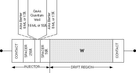
Fig. 3 Layer schematic of AlAs/GaAs Quantum Well Injection
Transit (QWITT) diode.
For purposes of analysis we decouple the semi-classical transport occurring
in the drift region from the quantum interference effects occurring in the
quantum well [36]. The influence of the drift region can then be understood
by characterizing the injector with an injection characteristic. This characteristic,
shown in Fig. 4, describes the current through the device as a function
of the electric field at the boundary separating the injector and the drift
region.
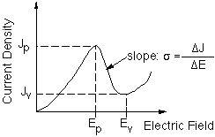
Fig. 4 Current density versus electric field (J - E) characteristics of
the DBRTD quantum well. Under the assumption that the drift region carrier
transport is at a constant saturation velocity, independent of the injection
characteristic, the J - E curve can be extracted from the DBRTD J - V characteristic
by accounting for the voltage drop due to the depleted spacer layers and
ohmic contact resistance.
Since the device is biased in the NDR region, the quantum well injector
can be characterized by a normalized injection conductance, sigma, which
is given by
 (20)
(20)
where the NDR characteristic was assumed to be linear between the peak and
valley.
We can now see how increasing the drift region or spacer layer width on
the anode side should affect  . Shown in Fig. 5 are the electric
field profiles in the drift region corresponding to the peak and valley
points of the J - E injector characteristic.
. Shown in Fig. 5 are the electric
field profiles in the drift region corresponding to the peak and valley
points of the J - E injector characteristic.
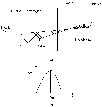
Fig. 5 (a) A qualitative illustration of the electric field profiles in
the drift region corresponding to the peak and valley points of the injector
characteristic of Fig. 4. W is the drift region length. The positive slope,
from Poisson's equation, represents the case where the injected electron
density necessary to support the current is less than the background doping.
(b) The voltage is just the shaded area between the peak
and valley electric field curves and is maximized at an optimum drift region
length, Wopt.
The slope of the electric field is positive, which from Poisson's equation,
represents the case where the injected electron density necessary to support
the current is less than the background doping density, as shown below
 (21)
(21)
where J is the current density through the device and Nd is the
background dopant concentration. The slope of the field at the valley is
greater than that at the peak because the current density, and thus the
electron concentration, is lower in the valley. The voltage , the difference
in the peak and valley voltages, is just the shaded area between the peak
and valley electric field curves. Therefore, by increasing W from the baseline
value of 250Å, one can increase the .
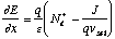
Quantitatively, the magnitude of the electric field as a function of position,
E1(z) at a constant current density J1 is:
 (22)
(22)
where Eo is the electric field at the injecting plane z = 0,
the boundary between the injector and the drift region. With a perturbation
in the form of additional current  , the resultant electric
field, E2(z) profile is given by
, the resultant electric
field, E2(z) profile is given by
 (23)
(23)
The corresponding change in voltage across the drift region to first order
in is then
 (24)
(24)
where W is assumed to remain the same before and after the current perturbation.
Dividing both side by , one arrives at an expression for
the differential resistance / across the drift
region:
 (25)
(25)
where
 (26)
(26)
Equation 25 is identical to Eq. 15, which was derived from the drift-diffusion
transport equations. This resistance is the ratio of the change in voltage
across the depletion layer to the change in current density.
Since it is desirable to operate the QWITT diode in the "low frequency"
limit where << , one can attempt to
maximize the negative resistance given by Eq. 25. For a given sigma and
vsat, the optimum drift region length, Wopt, for maximum
negative resistance is
 (27)
(27)
Wopt is the drift region length at which is maximum. From
Eq. 27, we see there are two ways to increase Wopt: decrease
sigma or increase vsat. By decreasing sigma, one reduces the
characteristic frequency, , and thus the frequency range
over which the negative resistance is constant. Increasing vsat
is possible by adjusting the material composition of the drift region. However,
lattice-matching requirements restrict the choice of drift region material
composition. AlAs/GaAs and AlAs/In0.53Ga0.47As QWITTs
require the drift region to be GaAs or AlGaAs and In0.53Ga0.47As,
respectively. Therefore, vsat is fixed by the drift region composition,
where the saturation velocity for GaAs and In0.53Ga0.47As
is 6 x 106 cm/sec and 5 x 106 cm/sec, respectively
[37, 38].
Figure 6 shows measured J - V characteristics for a baseline AlAs/In0.53Ga0.47As
DBRTD (W = 300Å) and an AlAs/In0.53Ga0.47As
QWITT with a drift region length of 1000Å. The emitter spacer layers
and quantum well in both devices are nominally identical. The quantum well
consists of 17Å AlAs barriers and a 50Å In0.53Ga0.47As
well. The emitter spacer layers, beginning with the closest to the quantum
well, are 50Å nominally undoped In0.53Ga0.47As
(n-type 5 x 1015 cm-3), 100Å (4 x 10¹⁶
cm-3) In0.53Ga0.47As, and finally 100Å
(2 x 1017 cm-3) In0.53Ga0.47As.
The for the baseline DBRTD is only 0.5 V. But by increasing
the drift length to 1000Å the is doubled to approximately
1.0 V. Since is increased while remains essentially
the same, the specific negative resistance increases over that of the baseline
DBRTD. This increased negative resistance relaxes circuit impedance matching
constraints and allows the use of larger area devices. Therefore much higher
RF output powers can be obtained
with QWITT diodes.
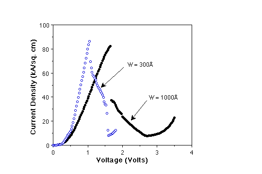
Fig. 6 Measured J - V characteristics of baseline AlAs/In0.53Ga0.47As
DBRTD with W=300Å and W=1000Å, AlAs/In0.53Ga0.47As
QWITT. The quantum well in both devices consists of 17Å AlAs barriers
and 50Å In0.53Ga0.47As well. The for the baseline
DBRTD and QWITT are 0.5 V and 1.0 V, respectively. The injection conductance,
sigma, for these devices is -0.5 (ohm-cm)-1. Since the has doubled while remains essentially the same, the
specific negative resistance is effectively doubled over that of the DBRTD.
Sponsors
This work was supported by the Texas Advanced Technology Research Program,
the Joint Services Electronics Program under contract AFOSR F 49620-86-C-0045,
and the National Science Foundation under grant ECS-8552868.
References
1. L.L. Chang, L. Esaki, and R. Tsu, "Resonant tunneling in semiconductor
double barriers," Appl. Phys. Lett., vol. 24, no. 12, pp. 593-595,
15 June, l974.
2. T.C.L.G. Sollner, W.D. Goodhue, P.E. Tannenwald, C.D. Parker, and D.D.
Peck, "Resonant tunneling through quantum wells at frequencies up to
2.5 THz," Appl. Phys. Lett., vol. 43, no. 6, pp. 588-590, 15 Sept.
1983.
3. T.C.L.G. Sollner, P.E. Tannenwald, D.D. Peck, and W.D. Goodhue, "Quantum
well oscillators," Appl. Phys. Lett., vol. 45, no.12, pp. 1319-1321,
Dec. 1984.
11. E.R. Brown, T.C.L.G. Sollner, W.D. Goodhue, and C.D. Parker, "Fundamental
oscillations up to 200 GHz in a resonant-tunneling diode," VIA-2, IEEE
Dev. Res. Conf., Santa Barbara, Calif., June 1987.
13. E.R. Brown, T.C.L.G. Sollner, W.D. Goodhue, and W.D. Parker, "Millimeter-band
oscillations based on resonant tunneling in a double barrier diode at room
temperature," Appl. Phys. Lett., vol. 50, no. 2, pp. 83-85, 12 Jan.
1987.
16. B. Ricco and M. Ya. Azbel, "Physics of resonant tunneling. The
one-dimensional double-barrier case," Phys. Rev. B, vol. 29, no. 4,
pp. 1970-1981, 15 Feb. 1984.
17. D.D. Coon, and H.C. Lui, "Frequency limit of double barrier resonant
tunneling oscillators," Appl. Phys. Lett., vol. 49, no. 2, pp. 94-96,
14 July 1986.
18. T.C.L.G. Sollner, E.R. Brown, W.D. Goodhue, and H.Q. Le, "Observation
of millimeter-wave oscillations from resonant tunneling diodes and some
theoretical considerations of ultimate frequency limits," Appl. Phys.
Lett., vol. 50, no. 6, pp. 332-334, 9 Feb. 1987.
19. P.D. Coleman, S. Goedeke, T.J. Shewchuk, P.C. Chapin, J.M. Gering, and
H. Morkoç, "Experimental study of the frequency limits of a
resonant tunneling oscillator," Appl. Phys. Lett., vol. 48, no. 6,
pp. 422-424, 10 Feb. 1986.
20. J.M. Gering, D.A. Crim, D.G. Morgan, P.D. Coleman, W. Kopp, and H. Morkoç,
"A small-signal equivalent-circuit model for GaAs-AlxGa1-xAs resonant
tunneling heterostructures at microwave frequencies," J. Appl. Phys.,
vol. 61, no. 1, pp. 271-276, 1 Jan. 1987.
21. B. Jogai, K. L. Wang, and K. W. Brown, "Frequency and power limit
of quantum well oscillators," Appl. Phys. Lett., vol. 48, no. 15, pp.
1003-1005, 14 April 1986.
22. V.P. Kesan, T.D. Linton, P.A. Blakey, D.P. Neikirk, and B.G. Streetman,
"Analysis of transit time effects due to spacer layers in quantum well
oscillators," Second Topical Conference on Picosecond Electronics and
Optoelectronics, Nevada, Jan 1987; to be published in Picosecond Electronics
and Optoelectronics, Springer Ser. in Electrophysics, Springer-Verlag,
1987.
23. V.P. Kesan, D.P. Neikirk, B.G. Streetman, and P.A. Blakey, "A new
transit-time device using quantum well injection," IEEE Elect. Dev.
Lett., vol. EDL-8, no. 4, pp. 129-131, Apr. 1987.
Also: V. P. Kesan, D. P. Neikirk, T. D. Linton, P. A. Blakey, and B. G.
Streetman, "Influence of Transit Time Effects on the Optimum Design
and Maximum Oscillation Frequency of Quantum Well Oscillators," IEEE
Trans. Electron Devices ED-35, April 1988, pp. 405-413.
24. M. Gilden, and M.E. Hines, "Electronic tuning effects in the Read
microwave avalanche diode," IEEE Trans. Elect. Dev., vol. ED-13, no.
1, pp. 169-175, Jan. 1966.
25. J.L. Chu, and S.M. Sze, "Microwave oscillations in pnp reach-through
BARITT diodes," Solid State Elect., vol. 16, pp. 85-91, 1973.
26. C. Yeh, "A unified treatment of the impedance of transit-time devices,"
IEEE Trans. Ed., vol. EE-28, no. 3, pp. 117-124, Aug. 1985.
30. C.I. Huang, M.J. Paulus, C.A. Bozada, S.C. Dudley, K.R. Evans, C.E.
Stutz, R.L. Jones, and M.E. Cheney, "AlGaAs/GaAs double barrier diodes
with high peak-to-valley current ratio," Appl. Phys. Lett., vol. 51,
no. 2, pp. 121-123, 13 July 1987.
31. W.R. Frensley, "Quantum transport calculation of the small-signal
response of a resonant tunneling diode," Appl. Phys. Lett., vol. 51,
no. 6, pp. 448-450, 10 Aug. 1987.
32. M.A. Reed, J.W. Lee, H.-L. Tsai, "Resonant tunneling through a
double GaAs/AlAs superlattice barrier, single quantum well heterostructure,"
Appl. Phys. Lett., no. 49, no. 3, pp. 158-160, 21 July 1986.
33. M. Cahay, M. McLennan, S. Datta, and M.S. Lundstrom, "Importance
of space-charge effects in resonant tunneling devices," no. 50, vol.
10, pp. 612-614, 9 March 1987.
34. K. K. Gullapalli, "Simulation of Electron transport in Double Barrier
Diodes," Master's Thesis, The University of Texas at Austin, Aug. 1991.
35. K. K. Gullapalli, A. J. Tsao, and D. P. Neikirk, "Observation of
zero-bias, multi-state behavior in selectively doped two-terminal quantum
tunneling devices," 1992 IEDM Digest, pp.479-482, 1993.
36. K. Gullapalli, V. K. Reddy, D. R. Miller and D. P. Neikirk, " Analysis
of Space Charge Effects in Resonant Tunneling Diodes," unpublished.
37. Sadao Adachi, " GaAs, AlAs, AlxGa1-xAs: Material parameters for
use in research anddevice applications," J. Appl. Phys., vol. 58, No.
3, pp.R1-R29, 1985.
38. T. H. Windhorn, L. W. Cook, and G. E. Stillman, " The Electron
Velocity-Field Characteristic for n-In0.53Ga0.47As at 300K," IEEE Electron
Device Lett., vol. 3, No. 1, 1982.