
Accurate measurement of the actual gap between the bearing pad and the runner is critical for accurate modeling and comparison with our experimental results. Presently, in the experimental set-up, we are using macroscopic proximity sensors, located at a few points at near the edge of the bearing pad. The need for integrated, in-situ proximity sensors has been stressed in the earlier reports. Previous work has led us to select inductive techniques using the principle of eddy-currents.
A two-coil transducer has been explored. Using Grover's [1] and Greenhouse's [2] model, values for the inductance of the coils have been calculated. Using these values a SPICE model has also been developed. The twin coil design avoids the problem of low Q in planar, small geometry spiral inductors. By measure a phase difference between input and output coils, the operating frequency remains largely insensitive to the resistance of the transducer.
Fabrication Issues
A schematic of the two-coil transducer is shown in fig. 1. As can be seen from the figure, we need to pattern at the bottom of the etched hole (on the back of the membrane) and along the sloping side-walls.
fig. 1
In order to test the coating properties of photoresist along the side walls of the hole, AZ5209 (0.9 um) photoresist was spun onto an etched hole. Figure 2 shows SEMs photomicrographs for the top and the bottom of the etched hole.
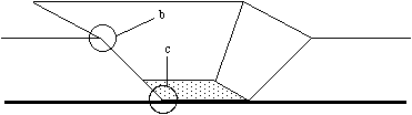
fig. 2a
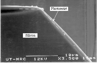
fig. 2b
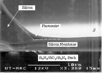
fig. 2c
As can be seen from the two SEMs, the photoresist is very conformal along the sidewalls and the bottom of the etched hole. The is a slight thinning of the photoresist at the top edge of the hole and also a slight thickening of the photoresist at the bottom edge of the hole.
Using the our Pattern/Mask Generator, a two-coil and single-coil direct write pattern has been drawn. Presently the fabrication process is being developed using a single coil direct-write pattern for test purposes. The Pattern Generator fractures the pattern drawn in AutoCAD and is capable of auto-focusing on the substrate before exposing each fracture. We plan to use this facility to expose connection lines along the side walls of the hole. Metallization using lift-off techniques has also been performed successfully. Since the developed photoresist profiles are not completely vertical there is a limitation to the thickness of the metal that can be deposited for lift-off to work. Tests were performed for different metal thicknesses. Up to 2700 Å of metal (130 Å Chromium, 2600 Å Silver) can deposited and lifted-off successfully for AZ5214E photoresist (1.4 um).

fig. 3
Shown in fig. 3 is the single-coil test inductor. The coil occupies a space of 1 mm2. The lines are 10 um wide with spaces of 10 um between segments, giivng a coil with 21 turns. Metal thickness is approximately 2700 Å as stated above. Polyimides (photo-definable and regular) are being examined for use as inter-metal dielectrics needed for the second level metal "escape" leads from the center of the spirals.
Future Goals
1) Process development of polyimide layer and second layer metal.
2) Measurement of inductance and resistance for single-coil design and comparison to simulated values.
3) Lithography at the back of membrane.
4) Lithography along the side-walls of etched hole.
1. F. W. Grover, Inductance Calculations: Working Formulas and Tables. New York: D. Van Nostrand Company, Inc., 1946.
2. H. M. Greenhouse, Design of Planar Rectangular Microelectronic Inductors, IEEE Transactions on Parts, Hybrids, and Packaging, vol. 10, pp. 101, 2 1974.