This paper is abstracted from:
J. M. Lewis, D. P. Neikirk, and S. M. Wentworth, "Low growth temperature
GaAs microbolometers," 15th International Conference on Infrared
and Millimeter Waves, R. J. Temkin ed., Dec. 10-14, 1990, pp. 398-400.
Low growth temperature GaAs (LTGaAs) microbolometers
Jason M. Lewis*, Stuart M. Wentworth+, and Dean P. Neikirk
Microelectronics Research Center, Department of Electrical and Computer
Engineering
The University of Texas at Austin
Austin, Texas 78712
* current address: Texas Instruments, Dallas, TX
+ current address: Electrical Engineering Department, Auburn University,
Auburn, AL 39849
ABSTRACT
Microbolometers with a large negative temperature coefficient have been
fabricated using an epitaxial GaAs layer grown at low temperature (LTGaAs).
The detector elements used have potential in composite bolometer structures
where high dR/dT materials can be used without having to be impedance matched
to the antenna structure. The LTGaAs material exhibited a thermally activated
conduction mechanism (Ea ~ 0.3 eV) with temperature coefficients
of -0.05 K-1 and -0.02 K-1 at 110 K and 290 K respectively.
Thermal impedance calculations suggest that the negative temperature coefficient
produces filamentary electrical paths. Intrinsic dc detector responsivities
as high as 108 V/W have been extracted from I-V measurements.
1. BACKGROUND
Conventional microbolometers for use as far infrared detectors operate
by using a planar antenna to capture electromagnetic radiation which is
absorbed by a detector element attached to the antenna. A signal is caused
by a change in resistance of the detector element upon heating. In conventional
microbolometers, the detector element is electrically attached to the antenna
and must be impedance matched to it in order to absorb radiation. Bismuth
is generally used for this material because it is one of the few materials
whose resistivity allows for impedance matching to antennas with impedances
of 100 - 200 [Omega]. Composite microbolometers have also been demonstrated
[1] in which the temperature sensing
element is in close thermal contact, but is electrically isolated from the
antenna load. This design allows the use of materials which can be chosen
to maximize dR/dT of the detector element to achieve greater responsivities.
A higher responsivity would provide a much easier means of detecting low
power levels.
2. DETECTOR MATERIALS
Most metals have very similar temperature coefficients (alpha) of around
0.003, with a being defined as
 (1)
(1)
In general, metals with the highest resistivity will exhibit the highest
dR/dT. Tellurium (a semi-metal) is one of the few conductive elements with
a resistivity higher than bismuth, and has been used in composite bolometer
structures [1]. Ordinary doped semiconductors
are relatively insensitive to temperature changes, and intrinsic semiconductors
are difficult to fabricate in microbolometer form. One approach to finding
a practical material with a higher dR/dT is to use epitaxial GaAs which
is grown at much lower temperatures than normal (referred to as LTGaAs)
[2], [3].
This material, originally used to prevent back-gating in MESFETs2,
has a very high defect density because of its low temperature growth process.
It also exhibits a strong temperature dependent resistivity. Films with
excellent surface morphology can be grown epitaxially on semi-insulating
GaAs, which effectively provides an electrically insulating substrate.
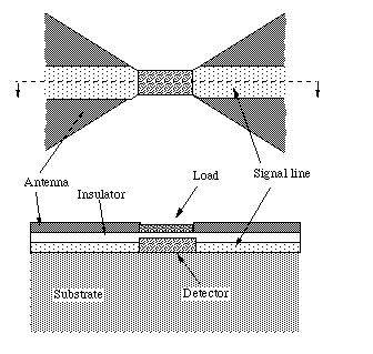
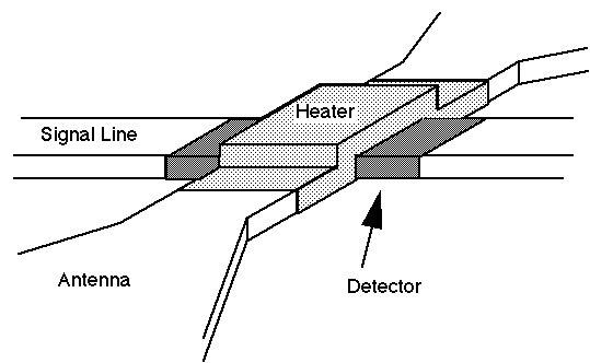
Figure 1: Bottom-view and cross-section of a composite microbolometer. The
load is impedance-matched to the bow-tie antenna, and is thermally coupled
to a detector.
Figure 2. Microbolometer with 10x10 um LTGaAs mesas. The gold bow-tie
antenna leads are shown with a mesa used as the detector element.
3. FABRICATION
For this study, conventional microbolometers were fabricated using LTGaAs
as a detector material between a bow-tie antenna structure. A 0.75 um layer
of LTGaAs was grown epitaxially on a semi-insulating (SI) GaAs substrate
at 270 C in an MBE system3. An antenna structure was evaporated
onto the LTGaAs layer and patterned by a bi-layer photoresist liftoff process
[4]. An electron beam was used to
evaporate 250 Å of Cr (for adhesion) followed by a 1500 Å layer
of gold for these antennas. The LTGaAs layer was then etched into 10x10
um square mesas which provided a small defined electrical connection between
the two antenna leads of each microbolometer. A micrograph of the resulting
structure is shown in Figure 2. Due to the pattern alignment, all LTGaAs
was removed between some bow ties, allowing a measurement of parasitic leakage
current through the SI GaAs substrate. For comparison, bow ties were also
fabricated directly on bare SI GaAs substrates.
4. MEASUREMENTS AND DISCUSSION
Current-voltage measurements (0 to 30 volts) were made at several temperatures
between 100 K to 340 K using an MMR low temperature probe station and an
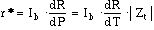
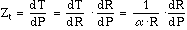
HP4140B. With this I-V-T data, resistance, intrinsic detector dc responsivity
r*, dR/dT, and thermal impedance Zt can be calculated. The intrinsic
responsivity is given by equations 2 and 3 :
 (2)
(2)
 (3)
(3)
where Ib is the bias current, R is the detector resistance, P
is the dc power (I.V) dissipated in the detector element, and Zt
is the thermal impedance for heat escaping from the detector element. dR/dP
and dR/dT can be extracted from the R-T and R-P data shown in Figure 3.
The actual bolometer temperature will rise above the ambient temperature
as the power increases. An estimation of the actual detector temperature
can be interpolated from Figure 3 and used to calculate (dT/dP), which is
the thermal impedance Zt. The intrinsic responsivity can also
be extracted using the values of dR/dP from Figure 3. Figure 4 shows the
thermal impedance and responsivity data extracted from Figure 3 for an ambient
temperature of 100 K.
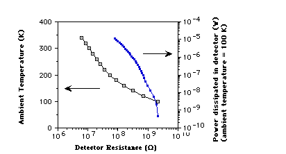
Figure 3: Detector resistance as a function of the power dissipated through
the LTGaAs element or ambient temperature. All temperature data points were
measured at 1 volt bias. The R-P curves cover bias voltages from 1 to 30
volts.

Figure 4: Intrinsic detector responsivity r* and thermal impedance as a
function of dissipated bias power.
The R-T characteristics closely follow a thermally activated conduction
mechanism with an activation energy of 0.03 eV. The temperature coefficients
at 100 K and 300 K were -0.05 K-1 and -0.02 K-1 respectively.
Measurements on bow ties without LTGaAs mesas connecting them gave resistances
three orders of magnitude higher, and very small positive temperature coefficients.
Bare SI GaAs substrates behaved in a very similar manner.
A rough approximation of the thermal impedance based on the LTGaAs mesa
geometry and material thermal properties is given by
 (4)
(4)
where [Kappa] is the thermal conductivity and A is the contact area between
the mesa and substrate[5]. This model
assumes heat flow into the substrate is the dominant heat sinking process.
By using the thermal conductivity of GaAs and assuming A to be the LTGaAs-GaAs
interface, this value of Zt is about 103 K/W (compared
to measured values of 105 - 109). This suggests that
heat flow is limited by a boundary that is much smaller than the size of
the LTGaAs mesa, and/or the thermal conductivity of the LTGaAs is very low.
The existence of thermal filaments[6]
could explain this phenomenon, in which the negative temperature coefficient
provides a low resistivity path through localized regions of heating.
The effects of filamentary current paths have uncertain consequences for
composite microbolometer operation. The thermal boundary caused by external
heating from the composite heater element (which governs actual composite
device responsivity) would be very different from the thermal filament boundaries
(which govern intrinsic dc responsivity). The larger thermal boundary may
reduce responsivity, but localized heating near the insulator interface
may help to enhance responsivity and speed. Assuming a thermal impedance
comparable to those achieved using tellurium detectors with NiCr heaters1,
a composite microbolometer responsivity of 5x10⁴ V/W might be
attained using LTGaAs detectors. Further research is currently under way
to evaluate the performance of such composite microbolometer structures.
4. ACKNOWLEDGEMENTS
This work was sponsored by the National Science Foundation under grant
number ECS-8552868. The authors would also like to acknowledge the assistance
of A. Tsao in sample preparation and etching.
5 REFERENCES
[1]. S.M. Wentworth and D.P. Neikirk,
"Far-infrared composite microbolometers," IEEE MTT-S Digest
1990, pp. 1309-1310.
[2]. F.W. Smith, A.R. Calawa, C. Chen,
IEEE Electron Device Lett 9, 1988, p. 77.
[3]. T.Y. Chu, A. Dodabalapur, D.P.
Neikirk, and B.G. Streetman, "Properties and applications of AlGaAs
grown at low temperatures," to be published in J. Crystal Growth,
1990.
[4]. D.M.Dobkin and B.D. Cantos, "Plasma
formation of buffer layers for multilayer resist structures," IEEE
Electron Device Lett., Vol. EDL-2, No. 9, Sept. 1981, pp. 222-224.
[5]. D.P. Neikirk, W.W. Lam, and D.B.
Rutledge, "Far-Infrared microbolometer detectors," Int. J.
Infrared and Millimeter Waves, Vol. 5, No. 3, 1984, pp 245-278.
[6]. E.C. Welks, R.M. Walser, R.W.
Bene', and W.H. Neal, "Response of thermal filaments in VO2
to produce laser-produced thermal perturbations," Appl. Phys. Lett.
vol 26, No. 7, 1 April 1975, pp 355-357.