FAR-INFRARED MICROBOLOMETER DETECTORS
by
STUART MARTIN WENTWORTH, B.S., M.S.
DISSERTATION
Presented to the Faculty of the Graduate School of
The University of Texas at Austin
in Partial Fulfillment
of the Requirements
for the Degree of
Doctor of Philosophy
THE UNIVERSITY OF TEXAS AT AUSTIN
May 1990
Copyright, May 1990 by STUART MARTIN WENTWORTH
Abstract
Stuart Martin Wentworth, Ph.D.
The University of Texas at Austin, 1990
Supervising Professor: Dean Paul Neikirk
Receivers and imaging systems for the far-infrared (FIR) spectral region (wavelengths between 100 µm and 3 mm) are desired for applications in astronomy, radar, and fusion research. Microbolometer detectors integrated with planar antennas are broad-band devices which work well in the FIR and which can be assembled into arrays for imaging. Radiation captured by the antenna heats the microbolometer detector, causing its temperature to change. With a good microbolometer material, this temperature change will result in a significant change in resistance, which can be measured. Also, a microbolometer has a small thermal mass, which means it can respond rapidly to a modulated FIR signal.
This study addresses the theory and operation of microbolometer detectors, and demonstrates the performance of conventional microbolometers using the elements bismuth and tellurium. The application of a bismuth microbolometer as the detector for a twin slot antenna structure is presented. The conventional microbolometer structure is constrained in that the resistance of the detector must match reasonably well with the impedance of the antenna. A composite microbolometer structure is demonstrated which removes this constraint. Finally, the sharp change in resistance at the transition temperature of a superconductor could be utilized to make a very responsive microbolometer. Preliminary results of such a transition edge microbolometer (TREMBOL) are presented using a conventional superconductor (lead) chilled to 7 K.
1. Introduction ..........................1
2. Microbolometer Theory ..........................8
2.1 Operation ..........................8
2.2 General Theory ..........................12
2.3 Noise ..........................20
2.4 Finite Element Thermal Model ..........................22
2.4.1 Steady State Case ..........................25
2.4.2 Time Dependent Case ..........................27
2.5 Bismuth Microbolometer ..........................30
2.6 Conclusions ..........................32
3. Materials, Structures, and Fabrication ..........................36
3.1 Bismuth ..........................36
3.2 Tellurium ..........................41
3.3 Microbolometer Fabrication ..........................42
3.3.1 Photoresist Bridge/Liftoff Process ..........................42
3.3.2 Vacuum Deposition ..........................47
3.4 Bismuth and Tellurium Microbolometers ..........................47
3.5 Composite Microbolometers ..........................50
3.5.1 Theory ..........................51
3.5.2 Fabrication ..........................52
3.5.3 Measurement ..........................54
3.5.4 Thermal Model ..........................58
3.5.5 Conclusions ..........................60
4. Twin Slot Antenna Structures ..........................65
4.1 Theory ..........................67
4.2 Fabrication ..........................71
4.3 Measurement ..........................75
4.4 Conclusions ..........................84
5. The Transition-Edge Microbolometer (TREMBOL) ..........................88
5.1 Background of Superconducting Bolometers ..........................88
5.2 The TREMBOL using a Conventional Superconductor ..........................90
5.3 The TREMBOL with Series-Added Resistance ..........................94
5.4 Composite TREMBOL ..........................97
5.4.1 Matrix Addressing in a Composite TREMBOL Array ..........................99
5.4.2 Capacitive Roll-Off in a Composite TREMBOL ..........................100
5.5 Cryogenic Apparatus ..........................103
5.6 Direction of Future Research ..........................105
A. Thermal Model for the Simple Microbolometer ..........................110
B. Routine Photolithography ..........................125
C. Electroplating ..........................126
D. CF4 Plasma Process ..........................128
E. STUVAC Operation ..........................131
Chapter 1
Introduction
Receivers and imaging systems for the far-infrared (FIR) spectral region (wavelengths between 100 µm and 3 mm) have received serious consideration only for about the last 20 years. Sensitive imaging detectors must still be developed for applications in astronomy, fusion research, and radar. In astronomy, interstellar medium emit energy mostly in the FIR spectral region. Observations made by the Infrared Astronomy Satellite (IRAS) have provided an enormous amount of new information on this cold luminous matter [], and within the next decade, more intensive study of this spectral region will be undertaken by the Space Infrared Telescope Facility (SIRTF), as well as by several other space-based facilities []. In fusion research, measurements of a plasma's electron density profile have been obtained by a FIR imaging system, using a novel bismuth microbolometer detector array []. A broader use of such detectors may be in the area of all-weather radar imaging systems for aircraft. Conventional microwave radar provides insufficient resolution for such applications, while optical systems have visibility restrictions in fog or clouds. A millimeter wave imaging system, however, would penetrate fog or clouds, while providing much higher resolution than conventional radar. This spectral region may also become important for the Strategic Defense Initiative []. Attenuation at high altitudes is low for this spectral range, so satellite-based submillimeter wave radar could detect high-flying objects, and with better resolution than conventional radar. Yet another benefit (hopefully never realized) is the excellent propagation of this type of radiation through nuclear debris. It is conjectured that high altitude nuclear bursts could be used to disrupt all communication signals under 60 GHz, but FIR communication would still be possible. As the sensitivity and speed of FIR detectors are improved, other applications will undoubtedly appear.
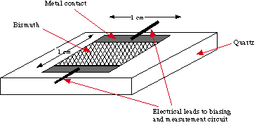
One type of detector that has been used extensively in the far-infrared (FIR) portion of the spectrum is the bolometer, which operates by changing resistance in response to a change in temperature. This temperature change is a result of radiation absorption. In order to efficiently absorb incident radiation the detector must be comparable in size to the wavelength l of the radiation, and be impedance-matched to free space. Conventional bolometers are typically several wavelengths square, which may be up to several square millimeters for longer FIR radiation. One such conventional bolometer is a millimeter and submillimeter power meter developed by Rebeiz et al.[], shown in Fig. 1.1. For this 1 cm2, 1000 Å thick bismuth bolometer biased at 1 V, a responsivity of 1 mV/W was obtained for a 100 Hz modulation frequency.
A drawback of these conventional-type bolometers is their large thermal mass, which reduces the speed at which they can respond to temperature changes. Also, the noise equivalent power (NEP), which should be as small as possible for sensitive operation, increases as the square root of this thermal mass. To improve bolometer performance for FIR applications the thermal detector must therefore be made as small as possible. One approach separates the radiation absorber from the
Fig. 1.1: A millimeter and submillimeter wave power meter using a conventional-type bolometer. Biased at 1 V, this 1000 Å thick bismuth film gave a responsivity of 1 mV/W for radiation modulated at 100 Hz.
temperature sensor. The absorbing material is chosen to efficiently capture the incoming radiation (and so must have an area of about l2), but can be relatively thin to give a low thermal mass. The temperature sensor material is chosen to produce very large changes in resistance with changing temperature, and must be in intimate thermal contact with the absorber, but may otherwise be very small. This composite structure can have an overall thermal mass which is much less than the conventional bolometer. A typical composite bolometer is shown in Fig. 1.2, where Bi is the radiation absorber and gallium-doped germanium is the temperature sensor [,]. This type of device has been used in astronomical applications []. Superconductors operating at their transition temperature have also been used in these composite structures [] and will be discussed further in chapter 5.
The above treatment views the radiation in an optical framework, as a source of energy that is passively absorbed by a surface. Another view is to treat the radiation as an electromagnetic wave which is captured and guided by an antenna. The antenna is also comparable in size to the wavelength, but does not dissipate any power. Instead, the antenna couples the power into a very small load resistor,
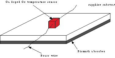
Fig. 1.2: This composite bolometer uses a bismuth radiation absorber in close thermal contact with a sensitive Ge:Ga temperature sensor. Thin brass wire is used as the signal and bias wire to minimize the thermal conduction pathway out of the sensor.
which is then the only part of the system to change temperature. A small device like this also has a large thermal impedance which results in a relatively large change in temperature for a given amount of dissipated power. If the load resistor is the bolometer itself, extremely fast and sensitive performance can result. Such a detector is called a microbolometer []. Antenna-coupled microbolometers have been shown to have higher responsivity, better sensitivity, and much faster response than conventional bolometers []. The theory and fabrication of these microbolometers will be discussed in chapters 2 and 3, respectively.
To make use of the approach discussed above, a FIR imaging system requires both an efficient antenna coupling structure as well as a sensitive detector. Much work has already been done to develop more efficient planar antennas [- ] which can be integrated with infrared detectors. Integrated circuit technology may be used to build arrays of such antennas and detectors, which are required for imaging applications []. At present, only two detectors have been integrated successfully with planar antennas to form imaging arrays: the planar Schottky diode, usually used for wavelengths longer than one millimeter []; and the room temperature microbolometer, which can be used throughout the FIR. Although Schottky diode detectors provide a significant advantage for mixer applications, their complexity of fabrication combined with their frequency limitations makes their use in the FIR difficult. Microbolometers, by contrast, are relatively simple to fabricate, and can be used with any type of dielectric substrate, allowing for more efficient antenna coupling at short wavelengths.
Both the high sensitivity and speed of the microbolometer, compared to other thermal detectors, is due to its small physical size: typically four micrometers square and 1000 Å thick (Fig. 1.3). If the bolometer material also has a large temperature coefficient of resistance a, defined as
a= 1/r dr/dT
where r is the resistivity and T is the temperature, high detector responsivities can be realized. In the past bismuth has been used almost exclusively as the detector material, with an a of only 0.003 K-1 [10]. It is clear that higher sensitivity would
be possible if some material with a larger value of a is used as the detector. In chapter 3, the use of tellurium (which has a steep dR/dT) as a microbolometer candidate will be investigated []. Also discussed in chapter 3 is the composite microbolometer, a novel device which alleviates the antenna impedance/load resistance mismatch problem.
A superconductor near its transition temperature has a very large temperature coefficient of resistance, in some cases over 0.50 K-1 []. Thus, if a microbolometer is fabricated with a superconducting thin film, and is operated near the transition edge, a dramatic increase in sensitivity may be realized. Such a device is called a transition-edge microbolometer, or TREMBOL, and will be discussed further in chapter 5.
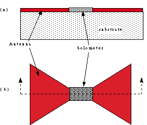
Fig. 1.3: Antenna-coupled microbolometer detector for FIR radiation detection: (a) cross section and (b) top view. The small size of the microbolometer makes it more sensitive, because its thermal impedance is higher than that for a conventional bolometer, and faster, because its thermal mass is smaller.